Semiconductor device and method for manufacturing the same

A semiconductor and device technology, applied in the field of semiconductor devices, can solve problems such as large data volume, uneven critical size, impossibility of rapid and accurate color filter design, etc.

Inactive Publication Date: 2008-11-12
DONGBU HITEK CO LTD
View PDF1 Cites 0 Cited by
  • Summary
  • Abstract
  • Description
  • Claims
  • Application Information

AI Technical Summary

Problems solved by technology

Due to this issue, the pattern's critical dimension (CD) may not be uniform
In addition, the patterning process of the color filter must be performed manually
Therefore, the amount of data required to design the pattern of the color filter is very large, making it impossible to quickly and accurately complete the design of the color filter

Method used


Image

  • Semiconductor device and method for manufacturing the same
  • Semiconductor device and method for manufacturing the same
  • Semiconductor device and method for manufacturing the same

Examples


Embodiment Construction

[0018] Reference will now be made in detail to the preferred embodiments of the invention, examples of which are illustrated in the accompanying drawings.

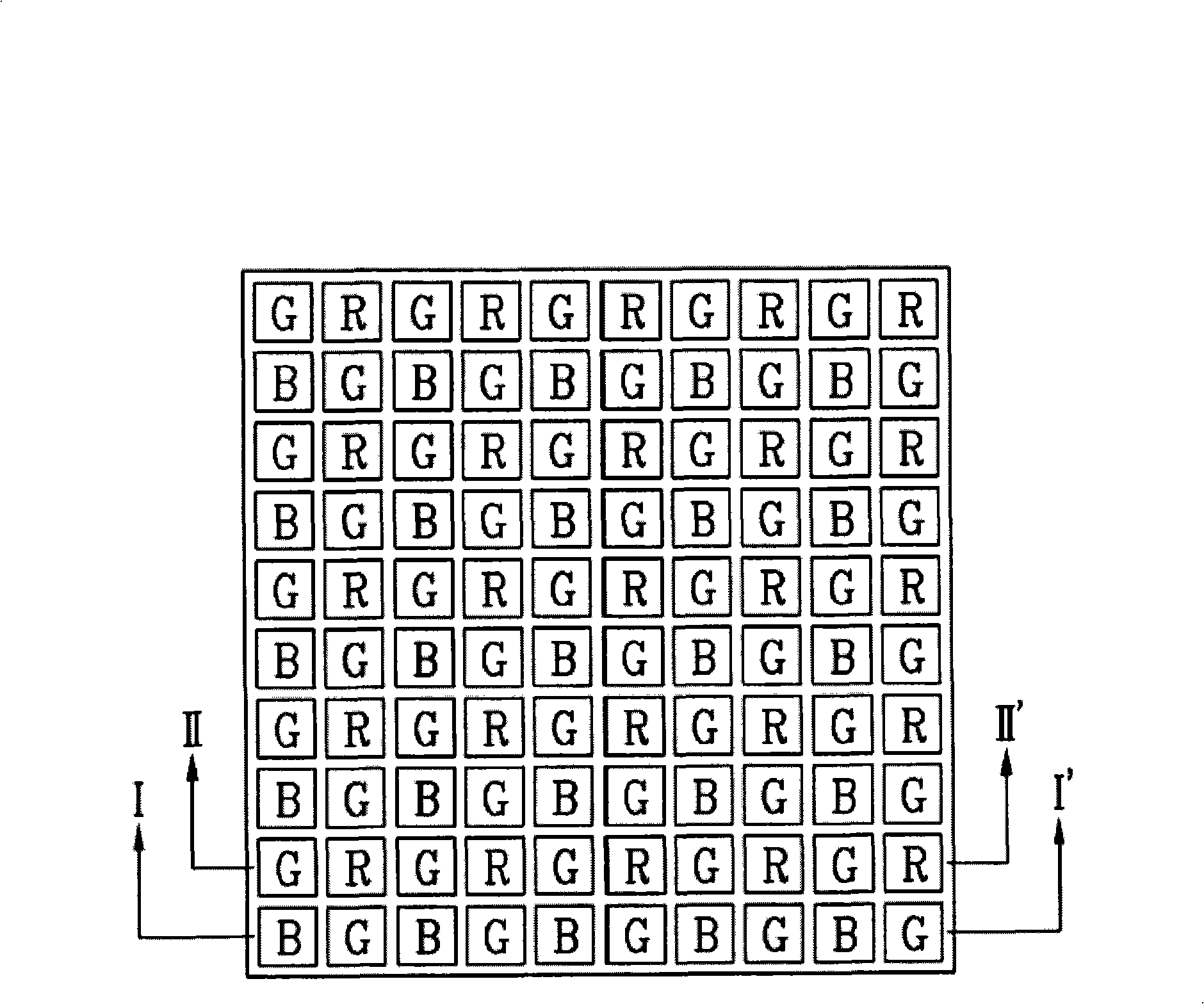
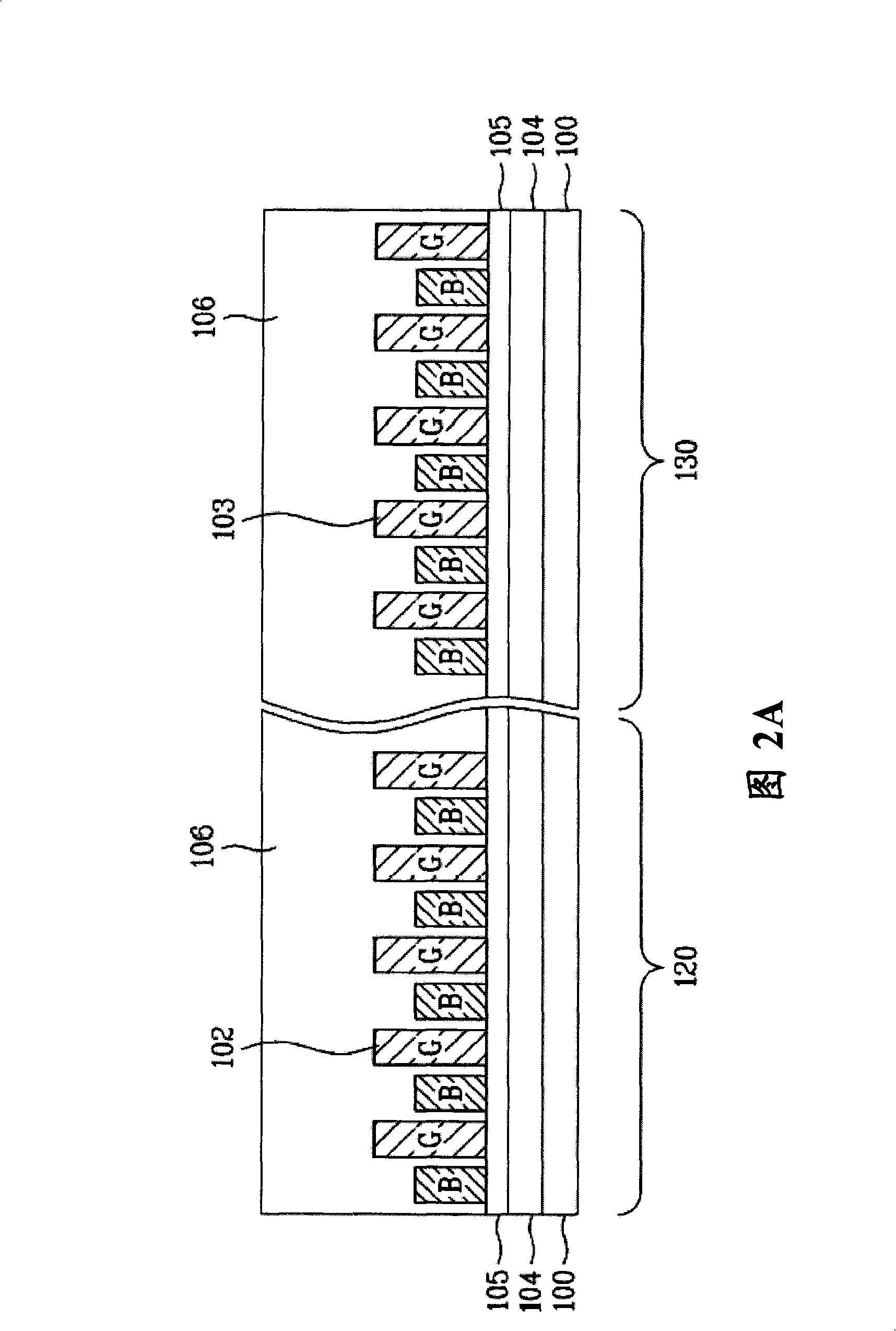
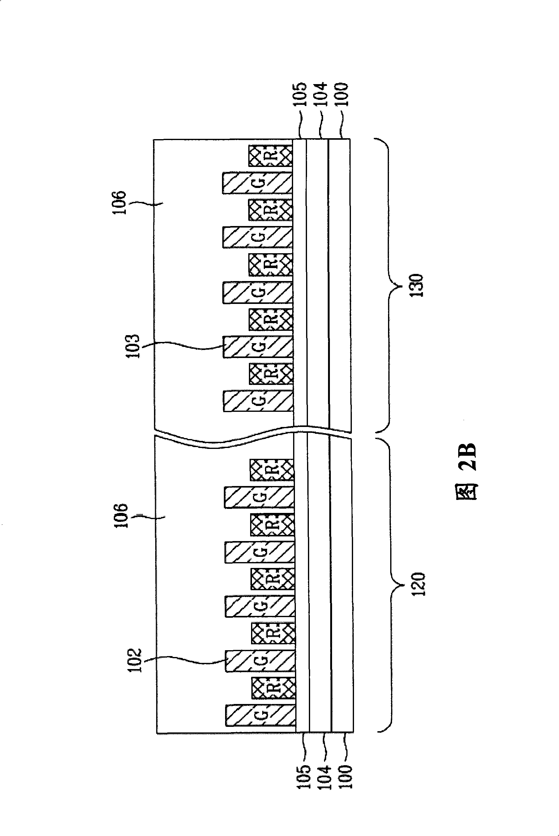
[0019] figure 1 is a plan view of a semiconductor device according to an exemplary embodiment of the present invention. 2A and 2B are cross-sectional views of a semiconductor device according to an exemplary embodiment of the present invention along section lines I-I' and II-II', respectively.

[0020] As shown in FIGS. 2A and 2B , the semiconductor device includes a dummy pattern area 120 and a main pattern area 130 for forming color filters. In Figure 2A, pass along the figure 1 The cross-sectional view of the semiconductor device taken along the line II′ in FIG. 1 shows the dummy pattern region 120 . In Figure 2B, pass along the figure 1 The cross-sectional view of the semiconductor device taken along the line II-II′ in FIG. 2 shows the dummy pattern region 120 .

[0021] refer to figure 1 2B, the semiconductor de...


PUM


Abstract

A semiconductor device and a method for manufacturing the same. The method includes setting a pattern region, forming a series of virtual mesh lines on the pattern region, forming a plurality of patterns in the pattern region, and substituting each of the patterns with either a red (R), green (G), or blue (B) patterns in accordance with a contact rule between the virtual mesh lines. Accordingly, it is possible to enhance the pattern uniformity between a main pattern region and a dummy pattern region, and thus to secure a uniform critical dimension (CD) of each pattern. Also, the patterning process for the color filter can be automatized to minimize the amount of data required to design a pattern. Also, the designing and manufacturing processes can be simplified, meaning that they can be more rapidly and precisely achieved.

Description

[0001] This application claims priority from Korean Patent Application No. 10-2007-0045623 filed on May 10, 2007, the entire contents of which are hereby incorporated by reference. technical field [0002] The present invention relates to a semiconductor device, and more particularly, to a semiconductor device and a method of manufacturing a semiconductor using a specific mask design. Background technique [0003] Generally, semiconductor devices have a multilayer structure in which the layers are formed using sputtering or chemical vapor deposition methods. These layers are then formed into a predetermined pattern in a subsequent photolithography process. [0004] Unfortunately, however, problems can arise in semiconductor devices due to variations in pattern size and / or density. In order to overcome these defects that have occurred, a technique has been developed in which a plurality of dummy patterns are formed together with a main pattern. [0005] However, when this t...

Claims


Application Information

Patent Timeline
Patent Type & Authority Applications(China)
IPC IPC(8): H01L21/82H01L27/146
CPCB29D11/00365G02B5/201H01L21/0274H01L21/0337
Inventor 李相熙曹甲焕
Owner DONGBU HITEK CO LTD
Why Eureka
Try Eureka