Semiconductor device and manufacturing method thereof

一种半导体、器件的技术,应用在半导体器件领域,能够解决不可能迅速且精确滤色器设计、数据量大、临界尺寸不均匀等问题

Inactive Publication Date: 2011-11-30
DONGBU HITEK CO LTD
View PDF1 Cites 0 Cited by
  • Summary
  • Abstract
  • Description
  • Claims
  • Application Information

AI Technical Summary

Problems solved by technology

Due to this issue, the pattern's critical dimension (CD) may not be uniform
In addition, the patterning process of the color filter must be performed manually
Therefore, the amount of data required to design the pattern of the color filter is very large, making it impossible to quickly and accurately complete the design of the color filter

Method used


Image

  • Semiconductor device and manufacturing method thereof
  • Semiconductor device and manufacturing method thereof
  • Semiconductor device and manufacturing method thereof

Examples


Embodiment Construction

[0018] Reference will now be made in detail to the preferred embodiments of the invention, examples of which are illustrated in the accompanying drawings.

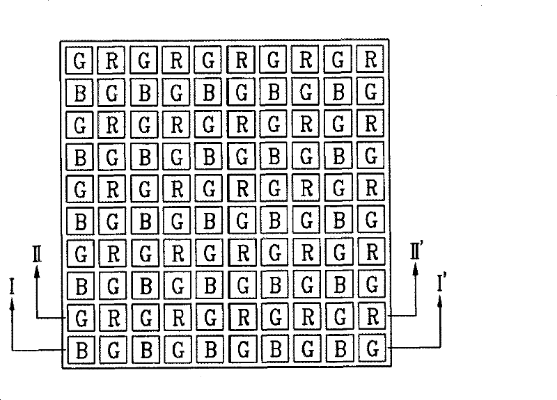
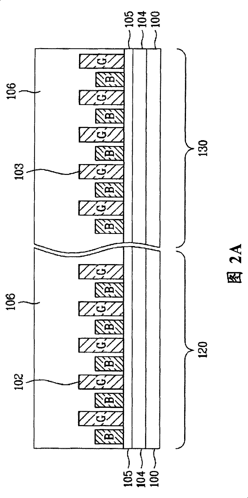
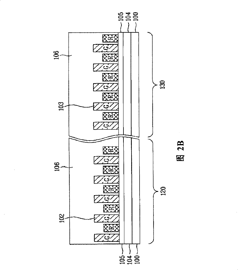
[0019] figure 1 is a plan view of a semiconductor device according to an exemplary embodiment of the present invention. Figure 2A and Figure 2B are cross-sectional views of semiconductor devices according to exemplary embodiments of the present invention along section lines II-I′ and II-II′, respectively.

[0020] like Figure 2A and Figure 2B As shown, the semiconductor device includes a dummy pattern area 120 and a main pattern area 130 for forming color filters. exist Figure 2A in, through the figure 1 The cross-sectional view of the semiconductor device taken along the line II′ in FIG. 1 shows the dummy pattern region 120 . exist Figure 2B in, through the figure 1 The cross-sectional view of the semiconductor device taken along the line II-II′ in FIG. 2 shows the dummy pattern region 120 .

[0021] refer...


PUM


Abstract

A semiconductor device and its manufacturing method. The method includes: setting a pattern area; forming a series of virtual grid lines on the pattern area; forming multiple patterns in the pattern area; and using red (R), green ( G), or blue (B) pattern to replace each pattern. Therefore, pattern uniformity between the main pattern area and the dummy pattern area can be improved, thereby ensuring a uniform critical dimension (CD) of each pattern. Also, the patterning process for color filters can be automated to minimize the amount of data required to design the pattern. Also, the design and manufacturing process can be simplified so that it can be realized quickly and accurately.

Description

[0001] This application claims priority from Korean Patent Application No. 10-2007-0045623 filed on May 10, 2007, the entire contents of which are hereby incorporated by reference. technical field [0002] The present invention relates to a semiconductor device, and more particularly, to a semiconductor device and a method of manufacturing a semiconductor using a specific mask design. Background technique [0003] Generally, semiconductor devices have a multilayer structure in which the layers are formed using sputtering or chemical vapor deposition methods. These layers are then formed into a predetermined pattern in a subsequent photolithography process. [0004] Unfortunately, however, problems can arise in semiconductor devices due to variations in pattern size and / or density. In order to overcome these defects that have occurred, a technique has been developed in which a plurality of dummy patterns are formed together with a main pattern. [0005] However, when this t...

Claims


Application Information

Patent Timeline
Patent Type & Authority Patents(China)
IPC IPC(8): H01L21/82H01L27/146
CPCG02B5/201B29D11/00365H01L21/0274H01L21/0337
Inventor 李相熙曹甲焕
Owner DONGBU HITEK CO LTD
Why Eureka
Try Eureka