Method of optical proximity correction for modifying line patterns and integrated circuts with line patterns modified by the same

a line pattern and optical proximity correction technology, applied in the field of optical proximity correction, can solve the problems of difficult design layouts having the critical dimensions for every component, the critical dimension required for semiconductor devices becomes smaller, etc., and achieve the effect of precise alignment of interconnect structures and uniform critical dimension of device patterns

Active Publication Date: 2014-10-09
UNITED MICROELECTRONICS CORP
View PDF20 Cites 9 Cited by
  • Summary
  • Abstract
  • Description
  • Claims
  • Application Information

AI Technical Summary

Benefits of technology

[0005]To meet the demand of reliable interconnections for nowadays semiconductor devices, a method of optical proximity correction is provided in the present invention which may modify the original layout pattern, such as a line pattern, to achieve a precise alignment of the interconnect structures between upper and lower layers while still maintaining the critical dimension uniformity (CDU) of the device pattern and providing a sufficient process window, ex. a PR window.

Problems solved by technology

However, as the scale of integration for nowadays electronic devices continues to shrink, the critical dimension (CD) required for semiconductor devices becomes smaller.
In this condition, it is quite difficult to design layouts having necessary critical dimensions for every component while still maintaining a precise alignment of the layouts and reliable interconnections between the conductive layers.

Method used


Image

  • Method of optical proximity correction for modifying line patterns and integrated circuts with line patterns modified by the same
  • Method of optical proximity correction for modifying line patterns and integrated circuts with line patterns modified by the same
  • Method of optical proximity correction for modifying line patterns and integrated circuts with line patterns modified by the same

Examples


Embodiment Construction

[0014]In the following detailed description of the present invention, reference is made to the accompanying drawings which form a part hereof and is shown byway of illustration and specific embodiments in which the invention may be practiced. These embodiments are described in sufficient details to enable those skilled in the art to practice the invention. Other embodiments may be utilized and structural, logical, and electrical changes may be made without departing from the scope of the present invention. The following detailed description, therefore, is not to be taken in a limiting sense, and the scope of the present invention is defined by the appended claims.

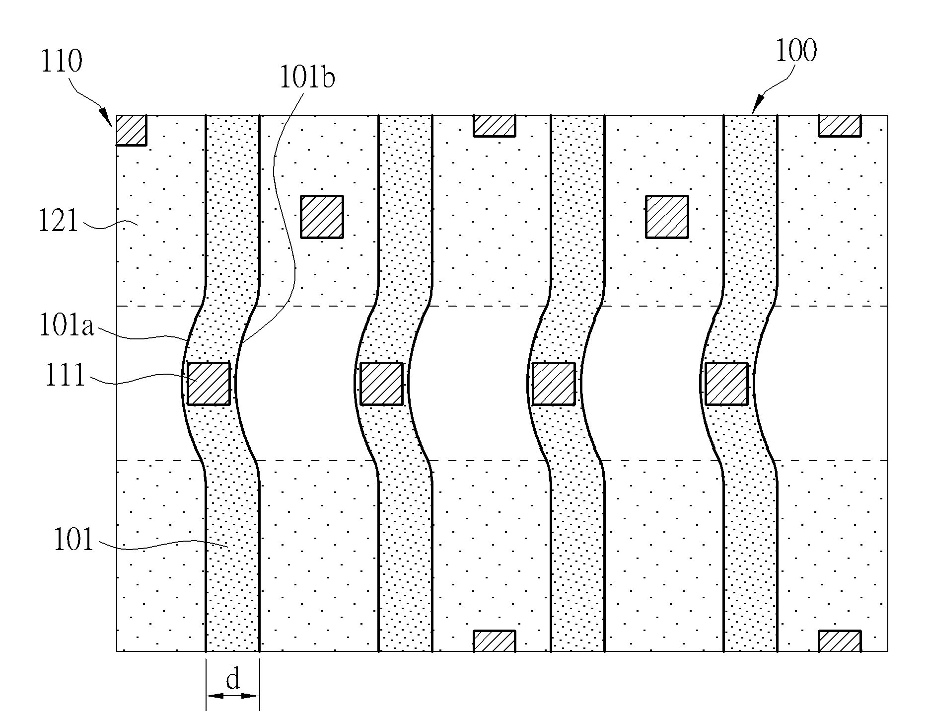
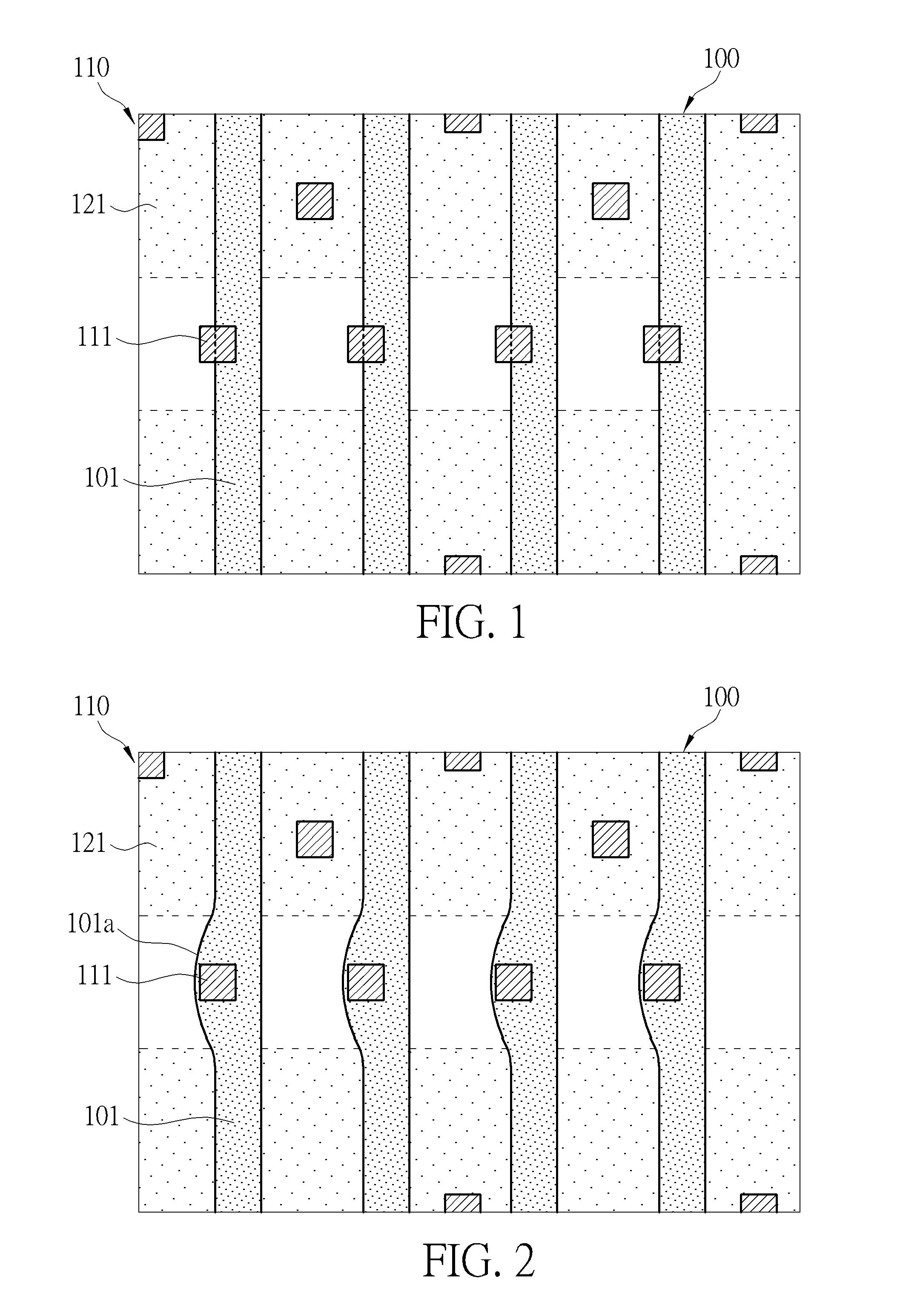
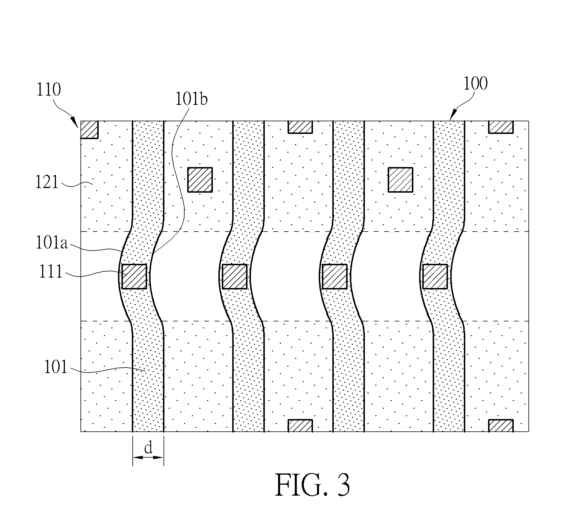
[0015]Please refer to FIG. 1, which schematically illustrates the deviation between an upper interconnect pattern and a lower interconnect pattern. Two stacked integrated circuit (IC) layouts are shown in FIG. 1, wherein one is a lower layout 100 denoted by dot patterns, and the other is an upper layout 110 denoted by hatch...


PUM


Abstract

A method of optical proximity correction executed by a computer system and integrated circuit layout formed by the same, the step of optical proximity correction comprises: providing an integrated circuit layout with a plurality of parallel line patterns, wherein one side of at least one line pattern is provided with a convex portion; and modifying the integrated circuit layout by forming a concave portion corresponding to the convex portion at the other side of the line pattern.

Description

BACKGROUND OF THE INVENTION[0001]1. Field of the Invention[0002]The present invention relates generally to a method of optical proximity correction (OPC), and more particularly, to a method of optical proximity correction capable of improving the coverage of inter-connect patterns stacked on line patterns.[0003]2. Description of the Prior Art[0004]In the fabrication of semiconductors, semiconductor devices are connected by multiple interconnect layers at different levels. Interlayer connections of various conductive layers are achieved by interconnection means such as vias or contacts. Accordingly, in the design of integrated circuit (IC) layout for each level, it is essential to consider the interconnect relation and the layout alignment of upper and lower levels as well as the limitations induced by process capability. However, as the scale of integration for nowadays electronic devices continues to shrink, the critical dimension (CD) required for semiconductor devices becomes sma...

Claims


Application Information

Patent Timeline
Patent Type & Authority Applications(United States)
IPC IPC(8): G06F17/50
CPCG06F17/5068G03F1/36H01L2924/0002H01L2924/00G06T2207/30148G06F30/39G06F30/394H01L23/5226H01L23/528H01L23/53271
Inventor FANG, KUAN-WENLIN, CHIN-LUNGTIEN, KUO-CHANGLEE, YI-HSIUWANG, CHIEN-HSIUNG
Owner UNITED MICROELECTRONICS CORP
Why Eureka
Try Eureka