Method for improving microspur consistency

A technology of critical size and consistency, which is applied in the direction of photolithography, optics, and instruments on the pattern surface. It can solve the problems of serious CD deviation, uneven etching of the center and edge of the wafer, and open circuit of the contact window, etc., to achieve uniformity. Critical dimension, the effect of improving the unevenness of the coating layer

Inactive Publication Date: 2005-03-30
WINBOND ELECTRONICS CORP
View PDF0 Cites 7 Cited by
  • Summary
  • Abstract
  • Description
  • Claims
  • Application Information

AI Technical Summary

Problems solved by technology

However, in the traditional manufacturing process, during the post-etching inspection (After Etching Inspection, AEI), it will be found that there is a deviation between the CD of the central part of the wafer and the CD of the edge part, and this deviation will cause some irreversible The lack of defects, such as the contact hole open circuit phenomenon obtained in the electrical acceptance test (Wafer Acceptance Test, WAT), these defects will seriously affect the pass rate
Now focus on the multi-layer coating film (multi-layer film), this multi-layer coating film due to more complex multi-layer coating and etching procedures, the transfer pattern formed after etching its central part and The CD deviation will be more serious at the edge
[0003] The main factors that lead to the CD deviation of the central and edge parts of the wafer are: first, the multi-layer coating film formed by spin-on-coating is caused by poor uniformity, refer to figure 1 The cross-sectional view of the multilayer film coated on the wafer substrate (substrate) 12, for example, is composed of an antireflection layer 14, a spin on glass (spin on glass, SOG) layer 16 and a photoresist layer 18 , the surface shape (topography) of the above-mentioned multilayer film in the central part 10 and the edge part 11 is as follows figure 1 The thickness shown is not consistent, the center is thin and the edge is thick. This kind of uneven coating is obviously not in line with the expected results in the case of multi-layer films; second, the current etching manufacturing process also often occurs in the center and edge of the wafer The phenomenon of uneven etching, the current technology is also unable to optimize the manufacturing process; third, even the substrate 12 formed by thin film deposition (such as figure 1 ) is not uniform enough to cause the result of CD deviation
[0004] For the above-mentioned CD deviation problem, for photolithography technology, although it is possible to adjust the settings of the exposure equipment, such as changing the ratio of the exposure dose to the exposure area, so that both the center and the edge of the wafer can obtain the desired CD target, However, even if efforts are made to improve the photolithography technology to suppress the CD deviation, after the etching process, the etching deviation still leads to the CD deviation in the center and the edge, which eventually causes irreparable defects.

Method used


Image

  • Method for improving microspur consistency
  • Method for improving microspur consistency
  • Method for improving microspur consistency

Examples


Embodiment Construction

[0044] In order to make the above-mentioned purposes, features and advantages of the present invention more obvious and understandable, according to the following Figure 2-1 to Figure 4-10 , especially give a preferred embodiment, and cooperate with accompanying drawing, describe in detail as follows:

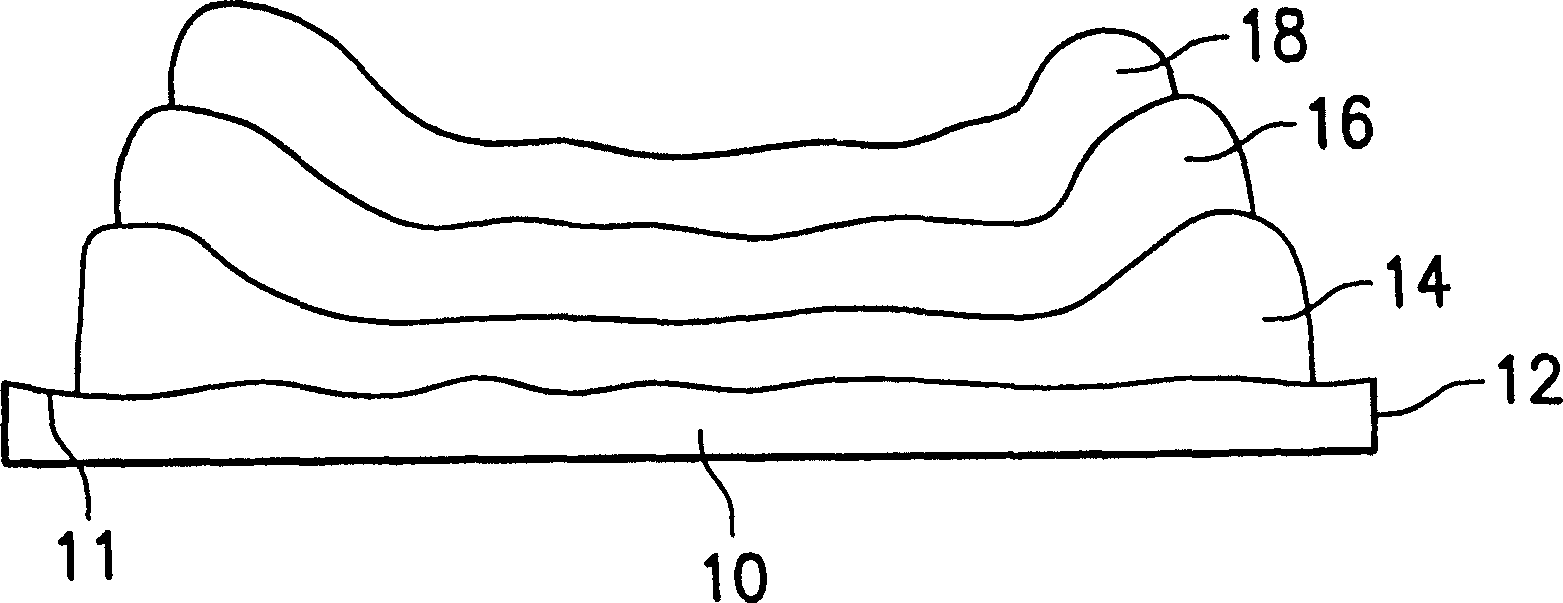
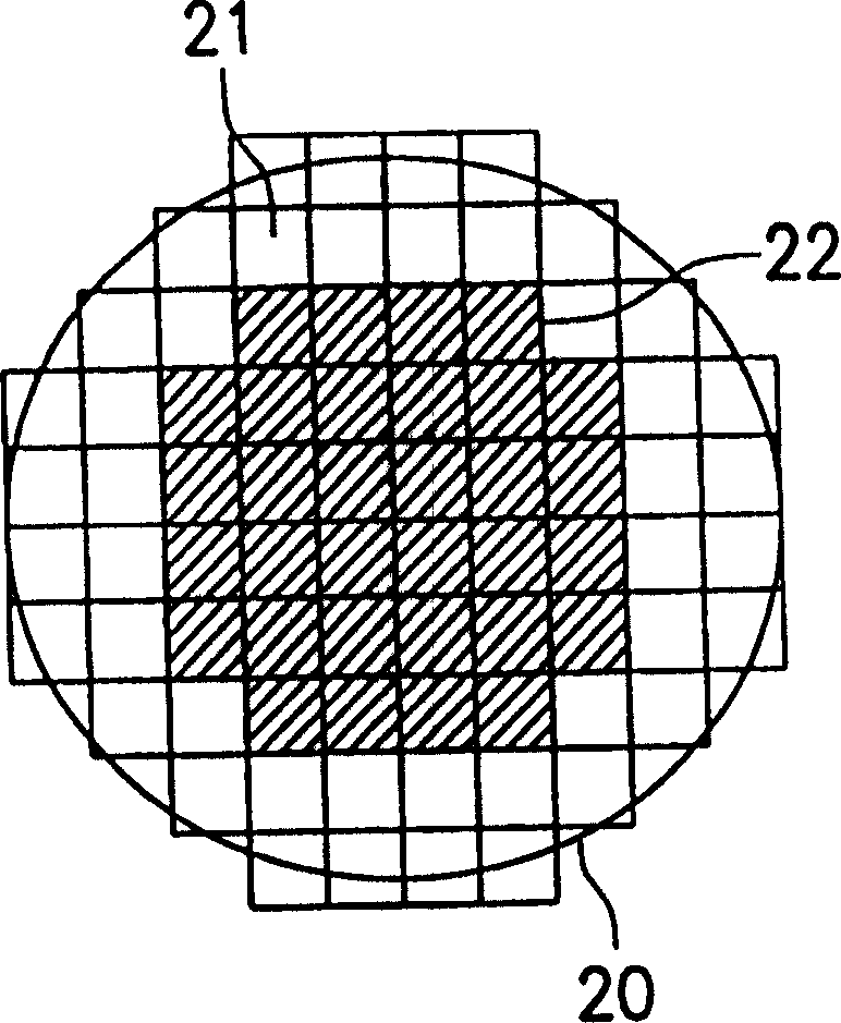
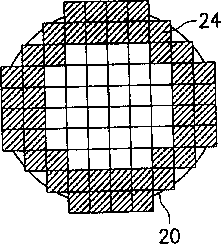
[0045] diagram 2-1, 2-2 is a schematic diagram of the first region 22 and the second region 24 defined in the embodiment described later, wherein the first region 22 and the second region 24 may not overlap each other, and the exposure on the wafer 20 The exposure field 21 is the range of one exposure in the stepping or scanning mode. refer to image 3 The flow chart of the embodiment of the present invention shown and the steps shown in the corresponding flow chart Figure 4-1 to Figure 4-10 ,in Pic 4-1 It is a schematic cross-sectional view of a wafer defining a part of the first region aa' and a part of the second region bb' in the embodiment:

[0046] First as step ...


PUM


Abstract

A method is suitable for manufacturing IC in order to overcome the inconsistency of microspurs between the center area and edge area caused by uneven thickness in center area and edge area on the coating layer coated on wafers. The pattern transfer manufacturnig procedure is carried out respectively in the invented method for the center area and the edge area by using special microfilm and etching techniques to reach the requirement of even microspurs for transferring pattern successfully. The center area and the edge area are not overlapped and their conditions of manufacturing procedures are set differently.

Description

technical field [0001] The present invention relates to a semiconductor manufacturing technology, in particular to a method for improving critical dimension uniformity by means of double-exposure and double-etch manufacturing procedures. Background technique [0002] In the semiconductor manufacturing process, lithography uses a step-by-step or scan-by-scan exposure procedure to expose a wafer (wafer) in sections to gradually complete the entire wafer. For the exposure of the wafer, the parameters that affect the lithography results must be fine-tuned and optimized before lithography. These lithography manufacturing process parameters include the thickness of the photo-resist (photo-resist), the temperature and time of baking / cooling, Development method and time, exposure dose, focal length compensation, and numerical aperture (Numerical Aperture, NA), etc. Next, etch is used to transfer the photoresist pattern (pattern) generated by the photolithography manufacturing proce...

Claims


Application Information

Patent Timeline
Patent Type & Authority Patents(China)
IPC IPC(8): G03F7/00H01L21/027H01L21/82
Inventor 徐义裕王国镇邵耀亭
Owner WINBOND ELECTRONICS CORP
Why Eureka
Try Eureka