

Physical operation method of flash memory chip
A technology of physical operation and flash memory chips, applied in the storage field, can solve the problem of low effective use capacity of flash memory chips
- Summary
- Abstract
- Description
- Claims
- Application Information
AI Technical Summary
Problems solved by technology
Method used
Image

Examples
Embodiment Construction
[0032] The present invention will be described in detail below in conjunction with the accompanying drawings and specific embodiments.
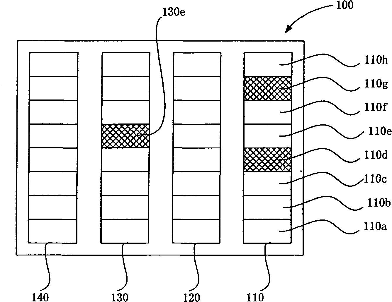
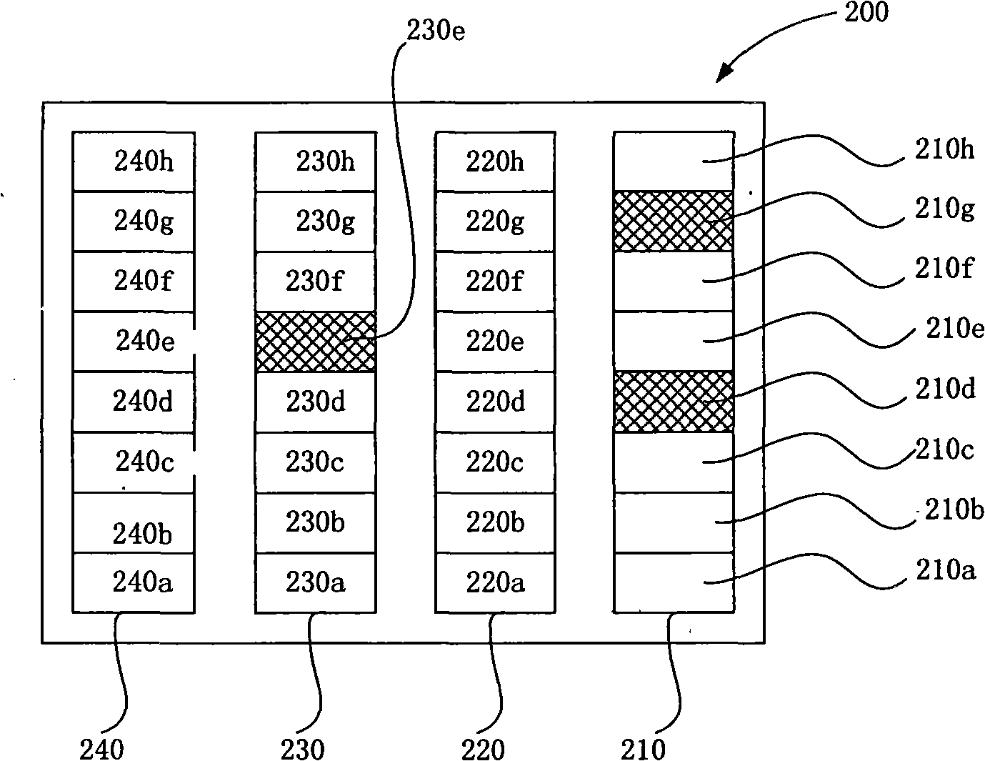
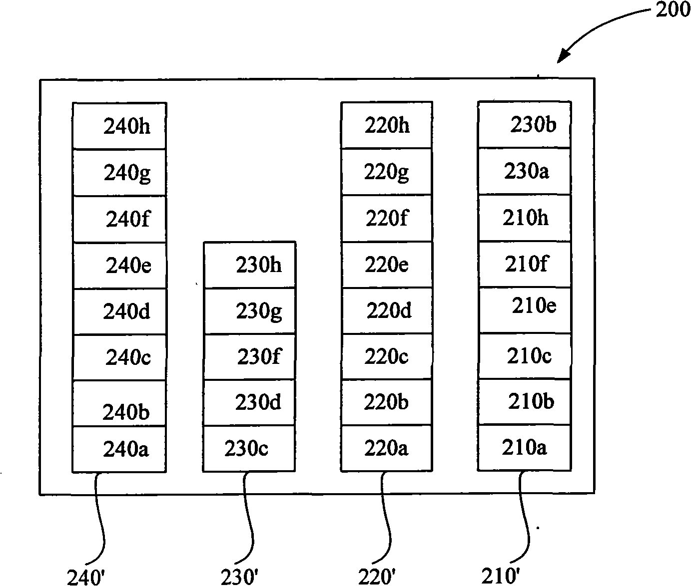
[0033] see figure 1 , is a schematic diagram of a flash memory chip 100 provided in the first embodiment of the present invention.
[0034] The flash memory chip 100 includes four memory blocks (Blocks), which are Block 110 , Block 120 , Block 130 and Block 140 . Each memory block has a block physical address. The block physical address may be the starting physical address of the storage block.
[0035] It can be understood that the flash memory chip 100 provided in this embodiment includes four memory blocks, which is not a limitation to the flash memory chip 100 of the present invention. Of course, the flash memory chip 100 can also include N memory blocks, and the N is greater than or an integer equal to 1.
[0036] In this embodiment, among the four storage blocks of the flash memory chip 100 , the storage block 110 and the storage bl...
PUM
 Abstract
Description
Claims
Application Information