Radiation detecting unit and radiation inspecting apparatus

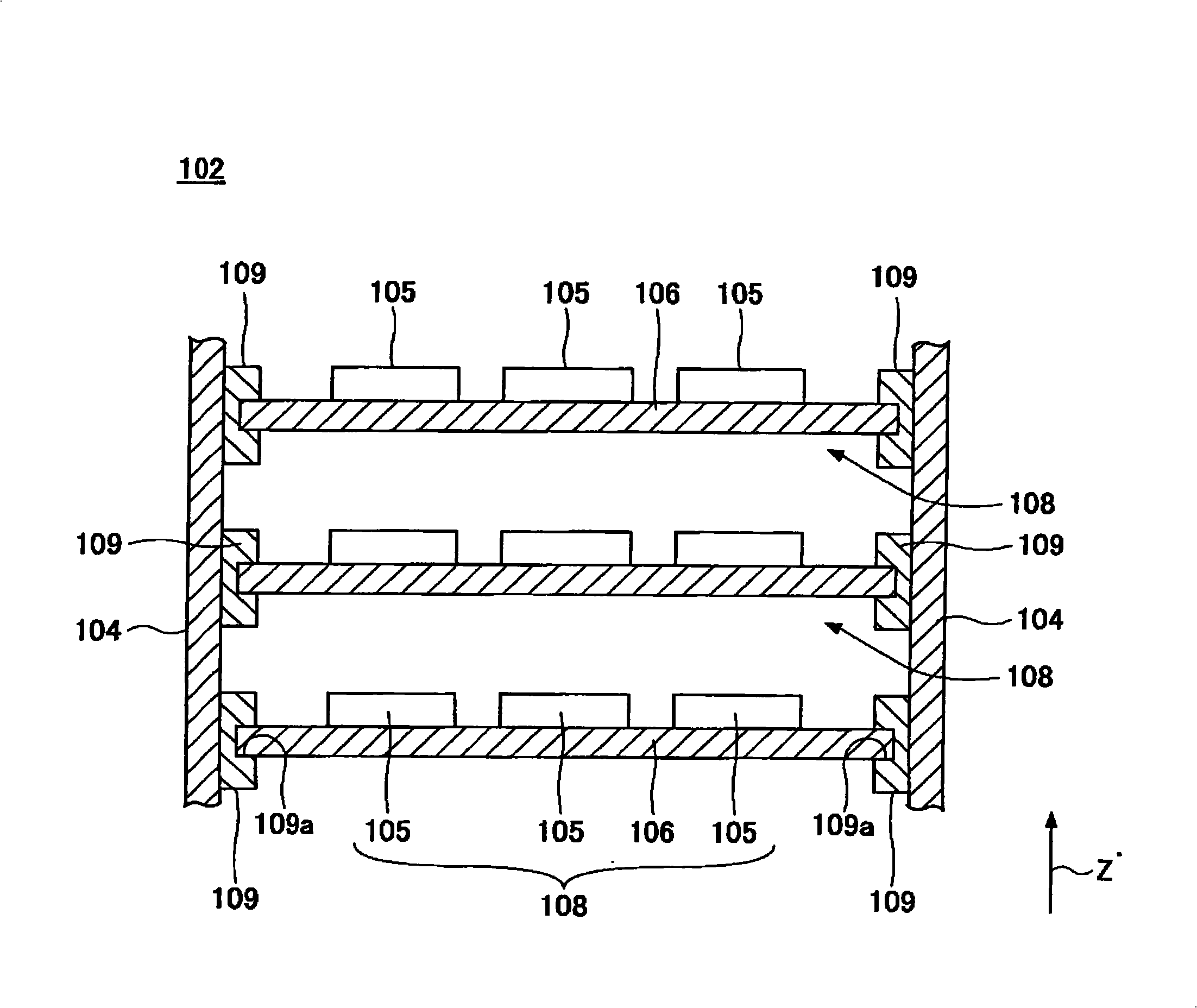
A radiation detection and inspection device technology, applied in the field of radiation detection units and radiation inspection devices, can solve the problems of the influence of the positioning accuracy of the semiconductor detection element 105, the difficulty in configuring the semiconductor detection element 105 with good accuracy, and the increase in the cost of the substrate 106, etc., to achieve Fine inspection, good precision, effect of improved spatial resolution

Inactive Publication Date: 2008-12-17
SUMITOMO HEAVY IND LTD
View PDF1 Cites 2 Cited by
  • Summary
  • Abstract
  • Description
  • Claims
  • Application Information

AI Technical Summary

Problems solved by technology

As a result, the cost of the substrate 106 increases
Furthermore, it also affects the positioning accuracy of the semiconductor detection element 105 with respect to the substrate 106.
[0007] In this way, there is a problem that it is difficult to arrange the semiconductor detection element 105 with high precision due to overlapping dimensional errors or positioning errors of the substrate 106 and the guide rail 109.

Method used


Image

  • Radiation detecting unit and radiation inspecting apparatus
  • Radiation detecting unit and radiation inspecting apparatus
  • Radiation detecting unit and radiation inspecting apparatus

Examples


Embodiment Construction

[0037] Referring to Figure 3 to Figure 19 Embodiments will be described.

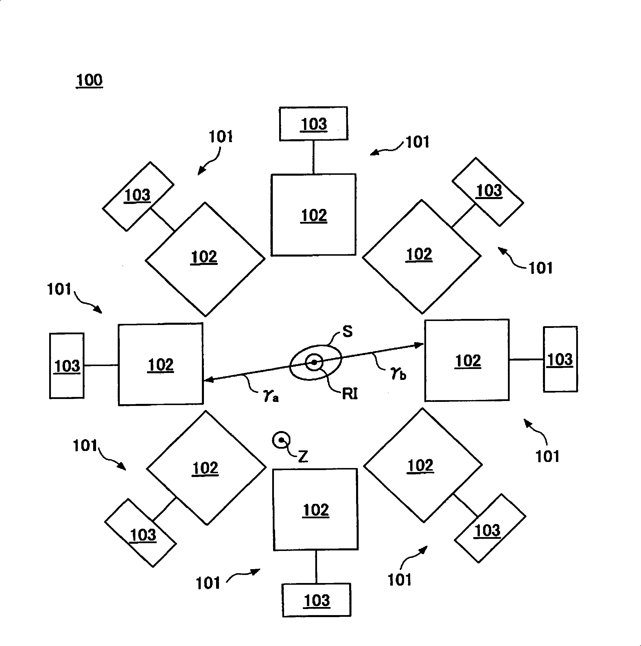
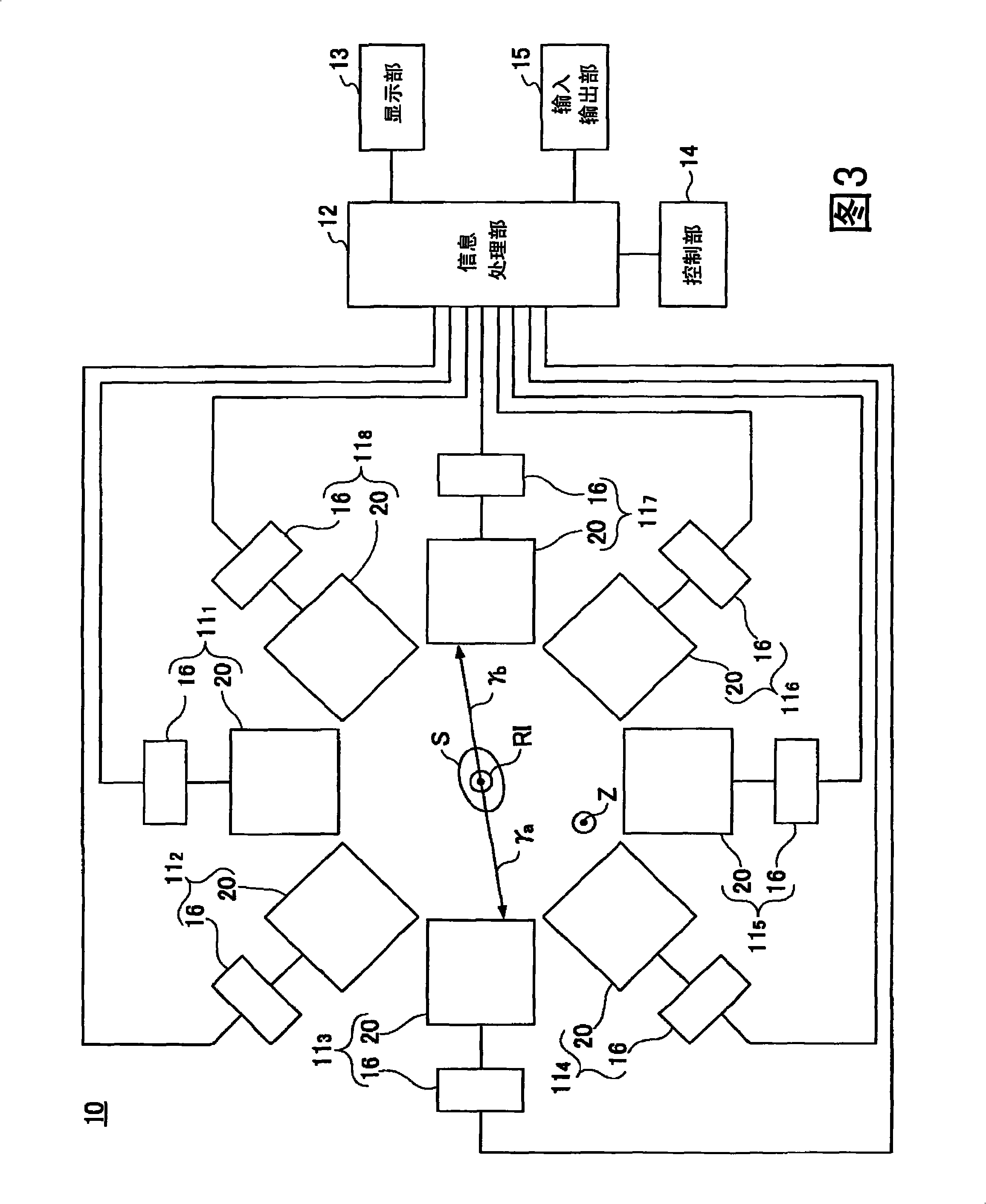
[0038] FIG. 3 is a block diagram showing the configuration of the PET apparatus according to the embodiment of the present invention. Referring to FIG. 3 , the PET apparatus 10 includes: a detector 11 arranged around the subject S to detect gamma rays; processing the detection data from the detector 11 to obtain positrons in the body of the subject S The information processing unit 12 for regenerating the position image data of the nuclide RI; the display unit 13 for displaying the image data; the control unit 14 for controlling the movement of the subject S or the detector 11; 12 or the input / output unit 15 composed of a terminal for sending instructions from the control unit 14 or a printer for outputting image data.

[0039] detector 11 1 ~118 Arranged within a range of 360 degrees around the subject S. Here, the body axis direction of the subject S is referred to as the Z-axis direction (Z and ...


PUM


Abstract

A detecting board (22) is provided with a wiring board (24), a semiconductor detecting element (25) firmly fixed on the upper plane of the wiring board (24) for detecting radiation and a spacer (28) firmly fixed on the upper plane of the wiring board (24), and a plurality of detecting boards are stacked and fixed. On each of the detecting boards (22), the semiconductor detecting element (25) and the spacer (28) are arranged to have a prescribed positional relationship. Furthermore, the detecting boards (22) are stacked by being aligned by the spacers (28) on an X-Y plane, and are fixed by fixing members (23a, 23b). The spacer (28) is provided with a step section (28e) so that the lower plane of the wiring board (24) is not brought into contact with the spacer (28) under the lower plane, and in the vertical direction, the spacers (28) are positioned by being brought into contact with each other.

Description

technical field [0001] The present invention relates to a radiation detection unit having a radiation semiconductor detection element and a radiation inspection apparatus using the same, and more particularly to a radiation detection unit and a radiation inspection apparatus for detecting gamma rays emitted from radioisotopes in a subject. Background technique [0002] In recent years, tomography apparatuses have been widely used to obtain information on the inside of a living body (subject). Examples of X-ray tomography devices include X-ray computed tomography (X-ray CT) devices, magnetic resonance imaging devices, SPECT (single photon emission CT) devices, and positron emission tomography devices. (PET) device. The X-ray CT device irradiates narrow X-ray beams to a section of the subject from multiple directions, and detects the transmitted X-rays, and then calculates the spatial distribution of the X-ray absorption degree in the section through a computer, so that pict...

Claims


Application Information

Patent Timeline
Patent Type & Authority Applications(China)
IPC IPC(8): G01T1/24H01L31/09G01T1/161
CPCG01T1/249G01T1/242H01L31/085
Inventor 浮田明宏
Owner SUMITOMO HEAVY IND LTD
Why Eureka
Try Eureka