Etching method

A technology for etching masks and etching equipment, applied in electrical components, semiconductor/solid-state device manufacturing, circuits, etc., can solve the problems of reducing product yield, etching rate changes, and different etching results, saving work. time, avoid the deviation of etching results, improve the effect of control

Active Publication Date: 2008-12-24
SEMICON MFG INT (SHANGHAI) CORP
View PDF1 Cites 14 Cited by
  • Summary
  • Abstract
  • Description
  • Claims
  • Application Information

AI Technical Summary

Problems solved by technology

[0003] Taking the etching process as an example, in the manufacture of integrated circuits, it is often necessary to use etching technology to form various etching patterns, such as contact hole / via pattern, trench isolation pattern or gate pattern, etc. If the above-mentioned etching pattern is caused by improper control The deviation of the characteristic dimension (CD, Critical Dimension) of the etching pattern will directly affect the performance of the circuit and reduce the yield of the product
[0004] However, in actual production, there are many factors that affect the etching results, which can be mainly divided into two categories: one is the impact of the previous process deviation before etching on the etching results, such as the material layer to be etched The difference in the deposition thickness, the difference in the CD of the etching mask pattern formed by lithography, etc. will cause the difference in the etching results.
The other is the influence of the etching process itself on the etching results. For example, when there are large differences in the size, shape and distribution density of the patterns to be etched on the substrate, the etching results will be different; in addition, there are It may be caused by unstable factors of the etching equipment itself. For example, after multiple etching processes, the environment in the working chamber of the etching equipment will change to a certain extent. This change will lead to changes in the etching rate, and the etching results will appear deviation

Method used


Image

  • Etching method
  • Etching method
  • Etching method

Examples


no. 1 example

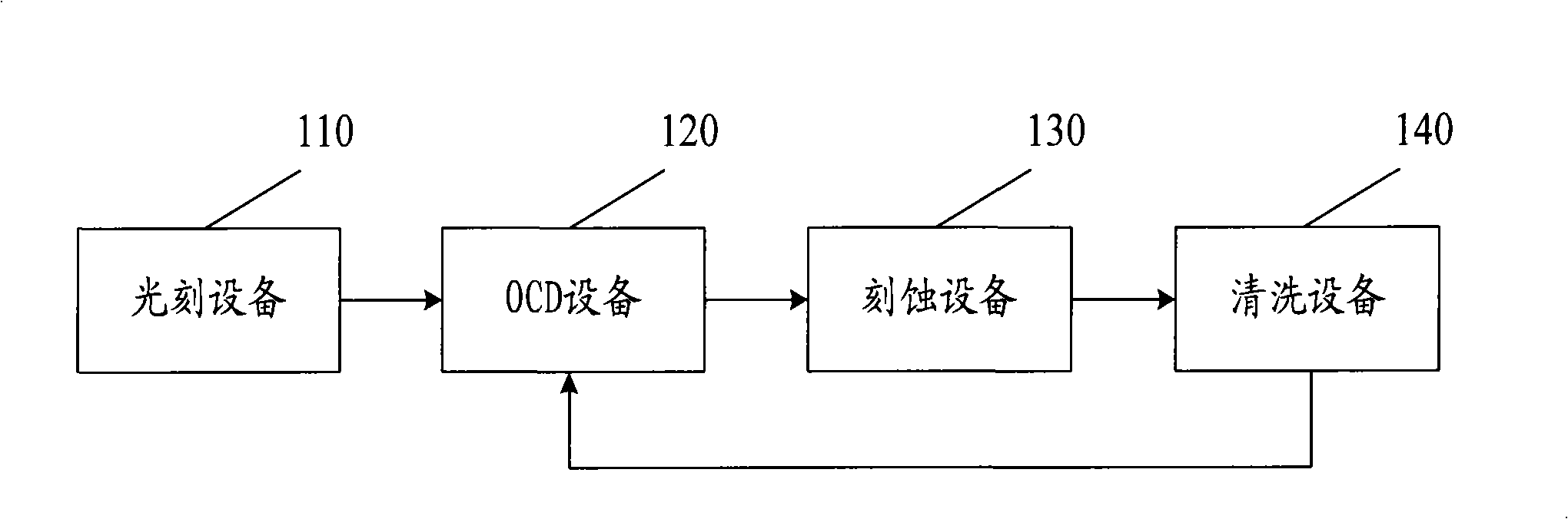
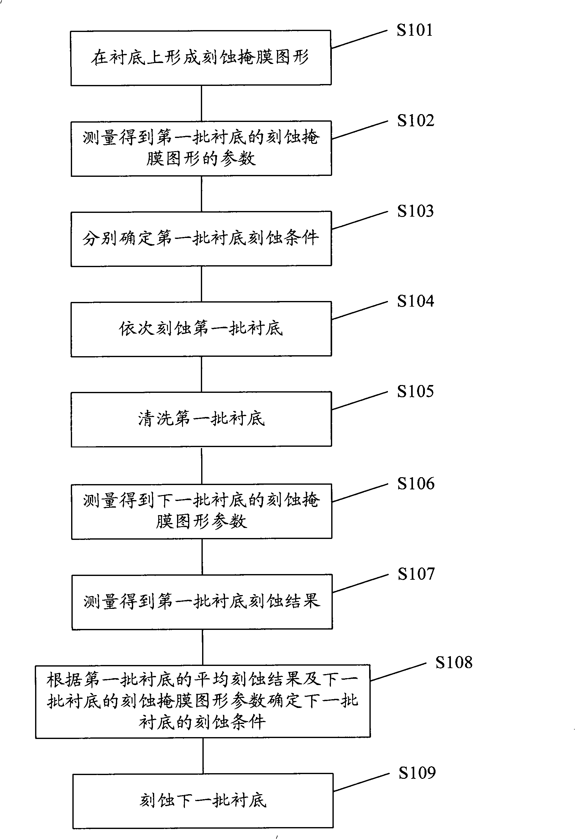
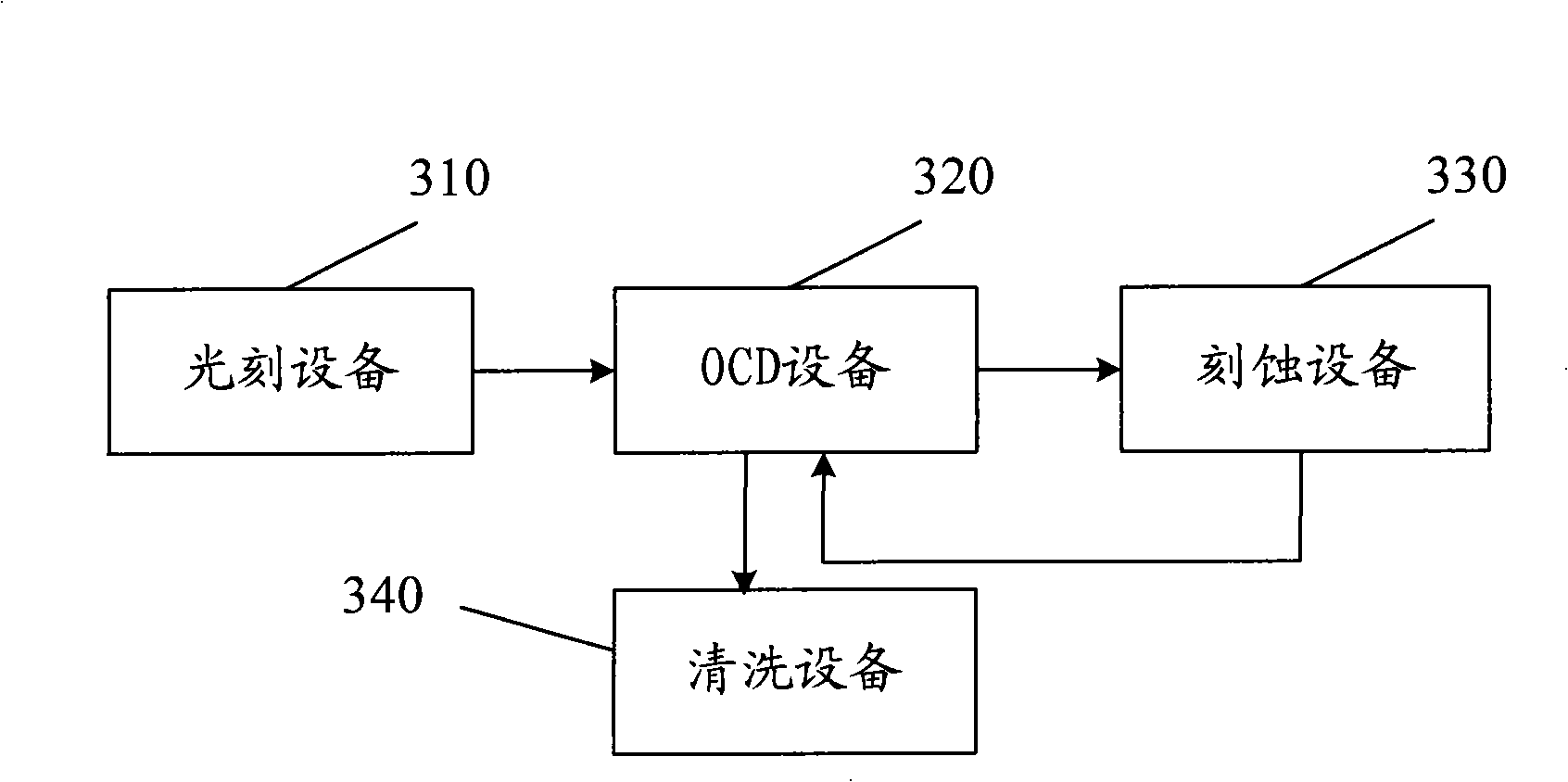
[0075] In actual production, each substrate is processed one by one during the photolithography, detection and etching process steps, and in cleaning, in order to save cost and time, it is usually cleaned in batches. For this reason, in the first embodiment of the present invention, each substrate is measured for the etched pattern CD before cleaning, and after a batch of substrates are etched, they are then uniformly sent to the cleaning device 340 for cleaning, which is the same as The traditional etching method is different (it measures the etched pattern CD after cleaning).

[0076] For this reason, it is necessary to verify that the measurement of the etched pattern CD performed before cleaning can also correctly reflect the state of the etching equipment. Figure 5 It is a comparison diagram of etching depth before / after cleaning in the first embodiment of the present invention, wherein the abscissa is the etching depth measured after cleaning, and the ordinate is the et...


PUM


Abstract

The invention discloses an etching method which includes the steps that a former substrate is etched; the etching mask pattern of a latter substrate is detected; the etching pattern of the former substrate is detected; according to the detection results of the etching pattern of the former substrate and the etching mask pattern of the latter substrate, the etching condition of the next substrate is determined; based on the etching condition of the latter substrate, the latter substrate is etched. The etching method of the invention can further improve the controlling force of an etching technology and the precision of etching.

Description

technical field [0001] The invention relates to the technical field of semiconductor manufacturing, in particular to an etching method. Background technique [0002] The integrated circuit manufacturing process is a planar manufacturing process that combines photolithography, etching, deposition, ion implantation and other processes to form a large number of various types of complex devices on the same substrate and connect them to each other to have a complete electronic functions. Among them, any deviation in the process may cause the performance parameters of the circuit to deviate from the design value. At present, with the continuous proportional reduction of the device feature size of VLSI and the continuous improvement of integration level, higher requirements are put forward for the control of each step of the process and the accuracy of the process results. [0003] Taking the etching process as an example, in the manufacture of integrated circuits, it is often ne...

Claims


Application Information

Patent Timeline
Patent Type & Authority Applications(China)
IPC IPC(8): H01L21/00H01L21/66
Inventor 黄怡杜珊珊朱峰张海洋
Owner SEMICON MFG INT (SHANGHAI) CORP
Why Eureka
Try Eureka