Address mappings method and operand parallel FFT processing system

An address mapping and processing system technology, applied in the field of FFT processing, can solve the problem that the processor cannot access operands in parallel

Inactive Publication Date: 2009-01-07
RDA MICROELECTRONICS SHANGHAICO LTD
View PDF0 Cites 24 Cited by
  • Summary
  • Abstract
  • Description
  • Claims
  • Application Information

AI Technical Summary

Problems solved by technology

[0013] It can be seen that for the butterfly operation of any N points above the second level, according to the existing address mapping method, there will be a situation where multiple operand addresses are located in the same memory bank, resulting in the processor being unable to access the operands in parallel.

Method used


Image

  • Address mappings method and operand parallel FFT processing system
  • Address mappings method and operand parallel FFT processing system
  • Address mappings method and operand parallel FFT processing system

Examples


example 1

[0064] In this example, the base-4 butterfly operation is used for illustration, taking 64 points as an example.

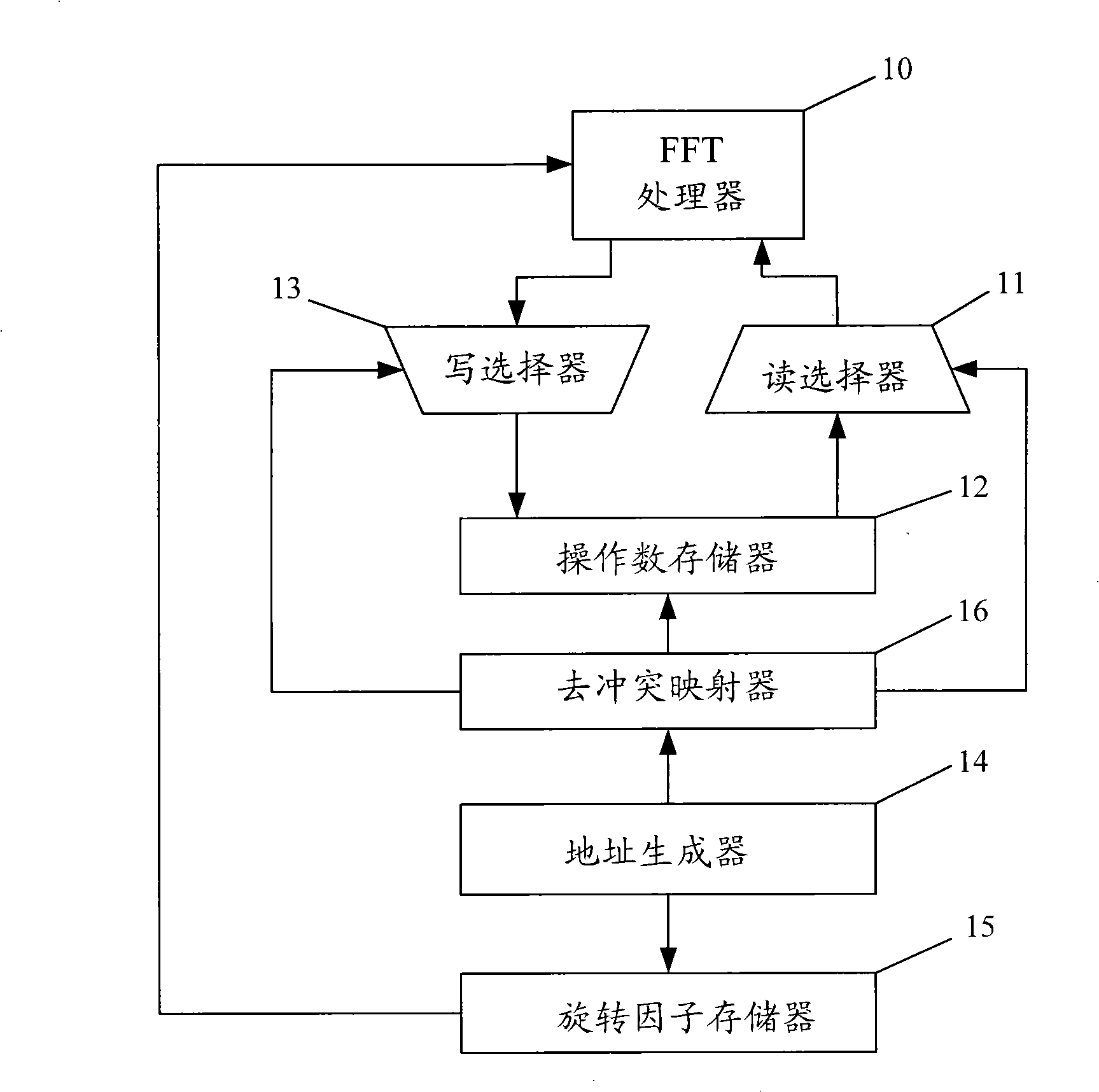
[0065] FIG. 3 is a schematic structural diagram of an FFT processing system with parallel operands of radix-4 butterfly operation. As shown in the figure, the operand memory 12 is composed of 4 memory banks of 0# memory bank 120, 1# memory bank 121, 2# memory bank 122 and 3# memory bank 123, so the slice address is at least two bits. Each storage bank has 16 storage spaces, correspondingly, each storage bank has 16 internal addresses, so the internal address has at least four bits. Therefore, in this example, the transmission lines connecting the decollision mapper 16 to each memory bank must be able to transmit at least 6-bit addresses in parallel.

[0066] The read selector 11 and the write selector 13 are 4 to 4 selectors respectively, and their design methods are in the prior art, and will not be repeated here. The read selector 11 and the write selector 13 ...

example 2

[0089] In this example, the radix-8 butterfly operation is used for illustration, taking 512 points as an example.

[0090] In this example, the first memory 12 includes 8 memory banks; both the read selector and the write selector are 8 to 8 selectors.

[0091] According to the existing address mapping method, in the 512-point radix-8 butterfly operation, the initial address is up to 9 bits, so the transmission line from the address generator 14 to the decollision mapper 16 can transmit at least 9 bits of address.

[0092] 512-point radix-8 butterfly operation, the operand memory 12 includes 8 memory banks, so the chip select address has at least 3 bits. The maximum internal address is 63, so the internal address must be at least 6 bits. Therefore, in this example, the transmission line connecting the decollision mapper 16 to each memory bank needs to be able to transmit at least 9-bit addresses.

[0093] Only the main differences between this example and Example 1 will be ...

example 3

[0125] This example is a mixed operation of radix 4 and radix 2 with 2048 points. The butterfly operation of 2048 points requires 1-level base 2 calculation and 5-level base 4 calculation; in actual processing, 5-level base 4 calculation can be performed after base 2 calculation; it can also be performed after 5-level base 4 calculation , and then do the base 2 operation.

[0126] In this example, the radix-2 operation is performed first as an example, but it does not show that the present invention is limited to this only. Those skilled in the art can easily transform it into performing 5-level radix-4 operations first, and then performing 1-level radix-2 operations.

[0127] In this example, Figure 3 is still taken as an example for illustration. The initial address of 2048 points is up to 11 bits. Compared with example 1, the difference of the FFT processing system with parallel operands mainly lies in that the transmission line connecting the address generator 14 and the ...


PUM


Abstract

The invention relates to an address mapping method and an FFT processing system with parallel operands. A primary address with a plurality of operands is generated at each time by the method, then the primary address is processed to generate a stack address and an inner address, wherein, the stack address is an address of a memory stack contained by a memory for storing the operands and the inner address is an address of all operands in all memory stacks; by adopting the address mapping method, the operands can be stored in different memory stacks, thereby ensuring that the operands can be in parallel in the butterfly-shaped operation. A collision removal mapper of the FFT processing system with the parallel operands is used for converting the primary address of the operands into a non-collision address, thereby ensuring that the operands can be stored in different memory stacks, and an FFT processor can access the operands in parallel so as to accelerate the operation speed.

Description

technical field [0001] The invention relates to FFT processing, in particular to an address mapping method of operands in butterfly operation and an FFT processing system for parallel access of operands. Background technique [0002] FFT (Fast Fourier Transformation, Fast Fourier Transformation) is one of the most important algorithms in digital signal processing applications. Whether it is frequency domain decimation (DFT) or time domain decimation (DIT), it can reduce the amount of calculation of FFT by eliminating redundancy. . Taking DFT as an example, the basic principle is: divide the data sequence into two sequences of equal length, convert the DFT of N points into two DFTs of N / 2 points, and repeat this process until the data sequence is decomposed into N / 2 2-point FFT, these points as the original data are reordered, N / 2 2-point DFTs take a pair of data for calculation, and these outputs are combined every 4 to perform N / 4 4-point DFT calculations; Then make appro...

Claims


Application Information

Patent Timeline
Patent Type & Authority Applications(China)
IPC IPC(8): G06F17/14
Inventor 周海峰曾珠峰
Owner RDA MICROELECTRONICS SHANGHAICO LTD
Why Eureka
Try Eureka