Multi-processor circuit with shared memory banks

A multi-processor, memory bank technology, applied in memory systems, electrical digital data processing, instruments, etc., can solve problems such as complex memory design

Inactive Publication Date: 2009-01-07
NXP BV
View PDF0 Cites 6 Cited by
  • Summary
  • Abstract
  • Description
  • Claims
  • Application Information

AI Technical Summary

Problems solved by technology

The use of caches also complicates memory design when compatibility between different caches must be maintained

Method used


Image

  • Multi-processor circuit with shared memory banks
  • Multi-processor circuit with shared memory banks
  • Multi-processor circuit with shared memory banks

Examples


Embodiment Construction

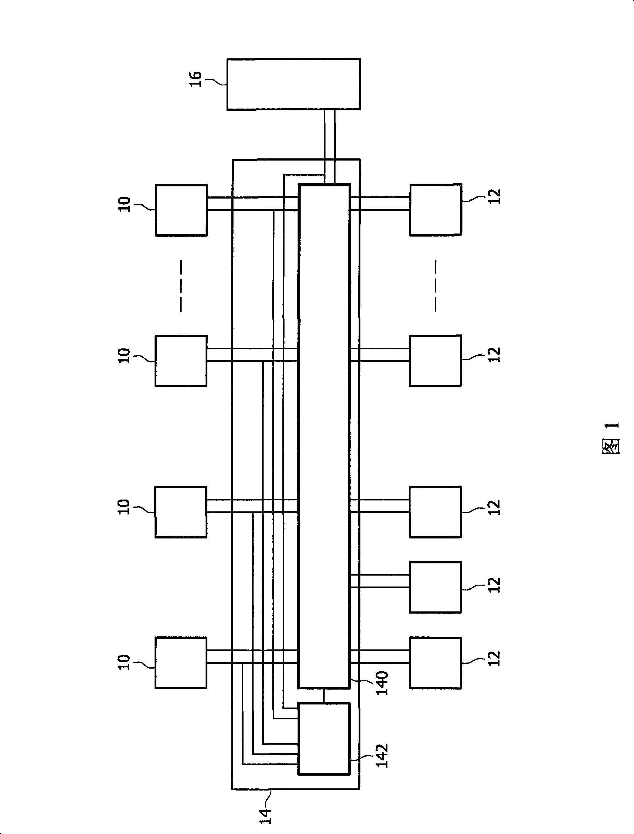
[0017] FIG. 1 shows a data processing circuit including a plurality of processors 10 , a plurality of memory banks 12 , connection circuits 14 and a disk defragmentation device 16 . The processor 10 and the disk defragmentation device 16 are coupled to the memory bank 12 through the connection circuit 14 . The connection circuit 14 includes a crossbar circuit 140 and an address arbiter 142 . The address output and data input / output of the processor 10 and the disk defragmentation device 16 are coupled to the crossbar circuit 140 . Address input and data input / output of memory bank 12 are coupled to crossbar circuit 140 . The address outputs of processor 10 and disk defragmentation device 16 are coupled to address arbiter 142, which has output terminals (only one shown) coupled to switch control inputs of crossbar circuit 140, and confirms processing input to device 10. Preferably, the disk defragmentation device 16 is coupled to the memory bank 12 as a processor similar to ...


PUM


Abstract

A plurality of processors (10) in a multiprocessor circuit is coupled to a plurality of independently addressable memory banks (12) via a connection circuit (14). The connection circuit is arranged to forward addresses from a combination of the processors (10) to addressing inputs of memory banks (12) selected by the addresses. The connection circuit (14) provides for a conflict resolution scheme wherein at least one of the processors (10) is associated with an associated one of the memory banks (12) as an associated processor. The connection circuit (14) guarantees the associated processor a higher minimum guaranteed access frequency to said associated one of the memory banks (12) than to a further one of the memory banks (12) other than the associated one of the memory banks (12). A defragmenter (16) detects data associated with a task running on the associated processor (10) that is stored on the further one of the memory banks (12) and move said data to the associated one of the memory banks (12) during execution of the task. The defragmenter causes addressing of the data by the associated processor (10) to be remapped from said further one of the memory banks (12) to the associated one of the banks after said moving, preferably incrementally as movement of data progresses.

Description

technical field [0001] The present invention relates to multiprocessor circuits. Background technique [0002] Memory access conflicts arise from problems with multiprocessor circuits. In a simple multiprocessor system, each processor is provided with its own memory bank that only it can access. Thus, no access conflicts will occur, however, the memory banks must be sized to support the most demanding tasks, implying considerable overhead for other tasks. Also, inter-processor communication cannot be performed through memory banks because these memory banks are only accessible to a single processor. [0003] An alternative is to use shared memory for all processors. However, this slows down multiprocessor systems in case of access conflicts. This problem can be alleviated by providing cache memories, where each cache memory is located between a respective processor and main memory. However, the cache memory greatly reduces the worst-case performance of the system (long ...

Claims


Application Information

Patent Timeline
Patent Type & Authority Applications(China)
IPC IPC(8): G06F13/16G06F13/18
CPCG06F12/0284G06F13/1652
Inventor 马尔科·J·G·贝库埃
Owner NXP BV
Why Eureka
Try Eureka