Modular transistor outline can with internal components

A device and photoelectric module technology, applied in the field of optical devices, can solve problems such as manufacturing difficulties and narrow error margins

Inactive Publication Date: 2009-01-07
FINISAR
View PDF2 Cites 20 Cited by
  • Summary
  • Abstract
  • Description
  • Claims
  • Application Information

AI Technical Summary

Problems solved by technology

However, TO-can size constraints have necessitated placement of optics and/or electronics outside of the header can
In turn, this setup causes other fabrication difficulties
For example, placing thes

Method used


Image

  • Modular transistor outline can with internal components
  • Modular transistor outline can with internal components
  • Modular transistor outline can with internal components

Examples


Embodiment Construction

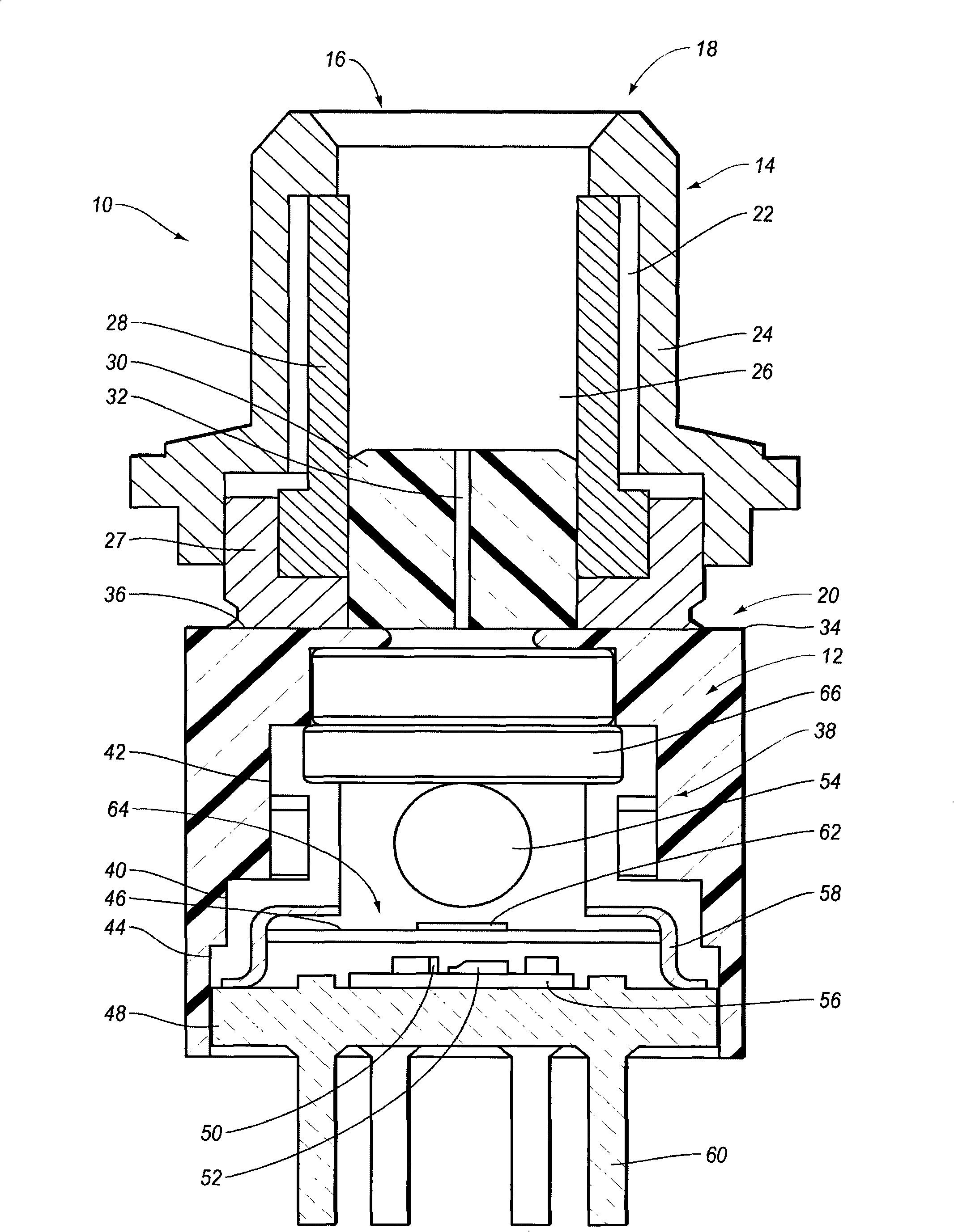
[0021] In general, embodiments of the present invention relate to optical packages, including header assemblies with various devices, suitable for use in TO-cans and related TOSAs.

[0022] In addition, embodiments of the invention relate to methods of fabrication of optoelectronic devices and devices, and methods of testing at various discrete stages of fabrication. Thus, as optoelectronic components, optoelectronic devices, and compact optical packages are assembled and manufactured, their reliability and / or functionality can be tested so that unreliable or non-working devices can be removed from the manufacturing process before many expensive devices are used. The relatively early days were abandoned or refitted. Simultaneous testing and manufacturing reduces the production cost of a functional optoelectronic data communication device.

[0023] I. optical components

[0024] Optical communication devices typically include optoelectronic transmitters that convert electri...


PUM


Abstract

The invention relates to a modular transistor outline can with internal components. In one example configuration, an optical package includes a substrate that supports a laser. The laser is configured for electrical communication with circuitry disposed on the substrate, and the laser is arranged to emit an optical signal along a first path. The optical package also includes a beam steering device supported by the substrate and arranged so as to receive the optical signal from the laser along the first path. The beam steering device is configured such that the optical signal is output from the beam steering device along a second path. A group of electronic leads is provided that electronically communicates with the circuitry on the substrate. In this example, the group includes a set of modulation leads in electrical communication with the laser, and a set of bias leads in electrical communication with the laser. The set of bias leads is electrically isolated from the set of modulation leads.

Description

technical field [0001] The present invention generally relates to optical devices having optoelectronic devices for data transmission, and more particularly, the present invention relates to optical assemblies comprising transistor outline (TO) cans having various internal devices. Background technique [0002] Recent trends in the advancement of optical data communications have resulted in smaller devices and faster data transfer rates. While inventors have succeeded in producing smaller and faster optoelectronic emitters, the reliability of smaller emitters has been problematic. In part, this arises from inherent problems associated with the complex fabrication techniques required to produce functionally reliable micro-emitters. Thus, as the size decreases, the percentage of inoperable micro-emitters increases. [0003] One consequence of increasing the likelihood of an optoelectronic emitter being inoperable is a drastic increase in manufacturing costs, which must be co...

Claims


Application Information

Patent Timeline
IPC IPC(8): H01S3/13H02B1/00
CPCH01S5/02438H01S5/02296H01S5/02212H01S5/02415H01S5/026H01S5/02292H01S5/02248H01S5/02284H01L2224/48091H01S5/0427H01L2224/49113H01L2924/30111H01L2224/05554H01S5/02325H01S5/02255H01S5/02251H01S5/02257H01L2924/00014H01L2924/00
Inventor 邓宏煜达里·J·度玛路易斯·B·阿朗森
Owner FINISAR
Why Eureka
Try Eureka