Inside imbedded type line board technique with conductive hole

A technology of embedded conductive holes, which is applied in the manufacture of multilayer circuits and the formation of electrical connections of printed components, etc. It can solve problems such as uneven distribution of contact stress, poor electrical connection quality between chips and circuit boards 100, and inability to bond chips. , to achieve good quality results

Active Publication Date: 2009-01-21
UNIMICRON TECH CORP
View PDF0 Cites 7 Cited by
  • Summary
  • Abstract
  • Description
  • Claims
  • Application Information

AI Technical Summary

Problems solved by technology

Wherein, since the thickness of the copper foil layer 114 and the conductive layer 130 made of copper such as copper have large variability during the formation process (that is, the surface of the patterned circuit layer 150 is relatively uneven), and the known technology cannot stably control Etching variability (the degree of etching of the copper foil layer 114 and the conductive layer 130 by the etchant), so the line width of the patterned circuit layer 150 produced by the known technology is difficult to meet the specifications of the thin line (the etchant will affect the copper foil layer 114 And the conductive layer 130 is over-etched so that the line width is difficult to meet the specifications of the thin line)
In other words, the known circuit board technology is not easy to produce circuit boards with fine lines
In addition, in the known technology, there is only one contact surface between the patterned circuit layer 150 and the dielectric layer 112, so the known patterned circuit layer 150 is easily peeled off from the dielectric layer 112 due to improper external force, resulting in circuit The reliability of the board 100 is reduced
[0005] In addition, in the subsequent chip packaging process, since the surface of the patterned circuit layer 150 is relatively uneven
Therefore, when the chip is arranged on the circuit board 100, the chip cannot be effectively bonded to the circuit board 100, resulting in poor electrical connection between the chip and the circuit board 100.
On the other hand, since the surface of the patterned circuit layer is uneven, when the chip is arranged on the circuit board 100, the contact stress distribution between the chip and the circuit board 100 is uneven, which in turn affects the reliability of the chip packaging structure.

Method used


Image

  • Inside imbedded type line board technique with conductive hole
  • Inside imbedded type line board technique with conductive hole
  • Inside imbedded type line board technique with conductive hole

Examples


Embodiment Construction

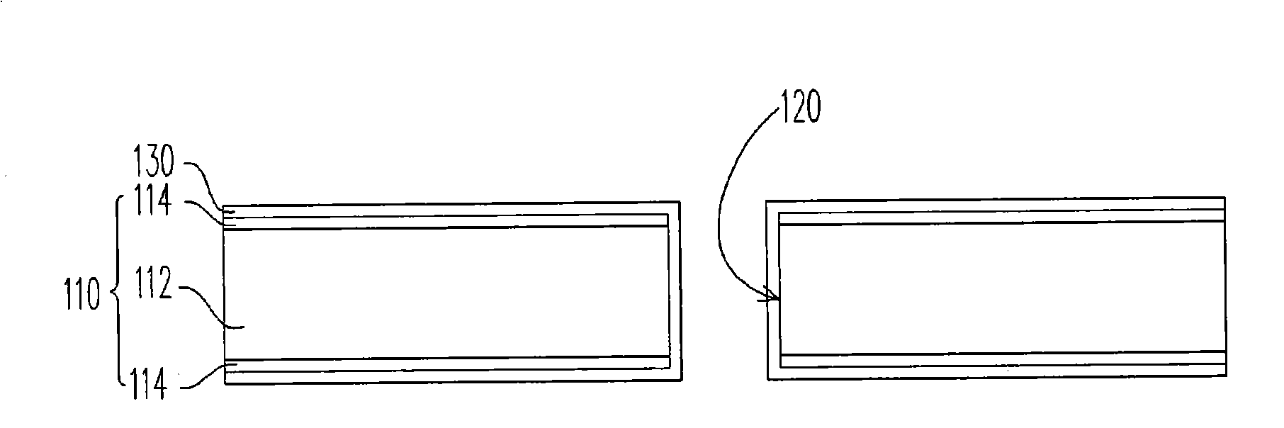
[0030] figure 2 A flow chart of manufacturing an embedded circuit board with conductive vias according to a preferred embodiment of the present invention is shown. Please refer to figure 2 , The embedded circuit board process of this embodiment includes the following steps: First, step S1 is performed to provide an embedded circuit board. Next, step S2 is executed to form openings on the embedded circuit substrate. Then, step S3 is executed to form a conductive layer on the first surface, the second surface and the inner wall of the opening of the embedded circuit substrate. Afterwards, step S4 is performed to remove the conductive layer on the first surface, the second surface and outside the opening to form a conductive hole. Hereinafter, this embodiment will illustrate the above circuit board process with a detailed process sectional view.

[0031] Figures 3A to 3E shown as figure 2 The process cross-section of the embedded circuit board with conductive vias. The...


PUM


Abstract

The invention discloses an embedded circuit board technology with conducting holes which comprises the following steps: firstly, an embedded circuit base plate is provided and the embedded circuit board comprises a dielectric layer, a first circuit layer and a second circuit layer, wherein, the dielectric layer comprises a first surface and a second surface, the first circuit layer is embedded in the first surface, the lateral surface of the first circuit layer has the same surface with the first surface, while the second circuit layer is embedded in the second surface and the lateral surface of the second circuit layer has the same surface with the second surface. Then an open hole forms in the embedded circuit base plate, and subsequently conducting layers form on the first surface, the second surface and the inner wall of the open hole. Finally, the conducting layers on the first surface, the second surface and the lateral side of the open hole are removed to form a conducting hole.

Description

technical field [0001] The invention relates to a circuit board process, and in particular to an embedded circuit board process with conductive holes. Background technique [0002] In recent years, with the rapid development of the production technology of the electronics industry, the circuit board (Circuit Board) can be equipped with various electronic components with exquisite volume, so as to be widely used in various electronic products with different functions. The manufacturing process of the known circuit board will be described below. Please refer to Figure 1A to Figure 1F , Figure 1A to Figure 1F It is shown as a cross-sectional flow diagram of a known circuit board process. Known circuit board technology comprises the following steps: at first, as Figure 1A As shown, a substrate 110 is provided. Wherein, the substrate 110 has a dielectric layer 112 and two copper foil layers 114 , and the dielectric layer 112 is disposed between the two copper foil layers 11...

Claims


Application Information

Patent Timeline
Patent Type & Authority Applications(China)
IPC IPC(8): H05K3/46H05K3/42
Inventor 陈宗源江书圣
Owner UNIMICRON TECH CORP
Why Eureka
Try Eureka