

Substrate transfer device, substrate processing apparatus and substrate transfer method
A handover device and substrate technology, applied in the direction of transportation and packaging, conveyor objects, electrical components, etc., can solve the problems of reducing wafer processing productivity and achieve the effect of improving productivity and rapid correction
- Summary
- Abstract
- Description
- Claims
- Application Information
AI Technical Summary
Problems solved by technology
Method used
Image

Examples
Embodiment Construction
[0060] Hereinafter, preferred embodiments of the present invention will be described in detail with reference to the drawings. In addition, in this specification and drawings, the same code|symbol is attached|subjected to the structural element which has substantially the same functional structure, and repeated description is abbreviate|omitted.
[0061] Substrate transfer device
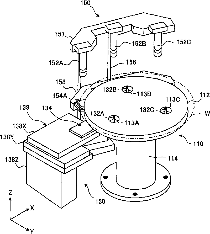
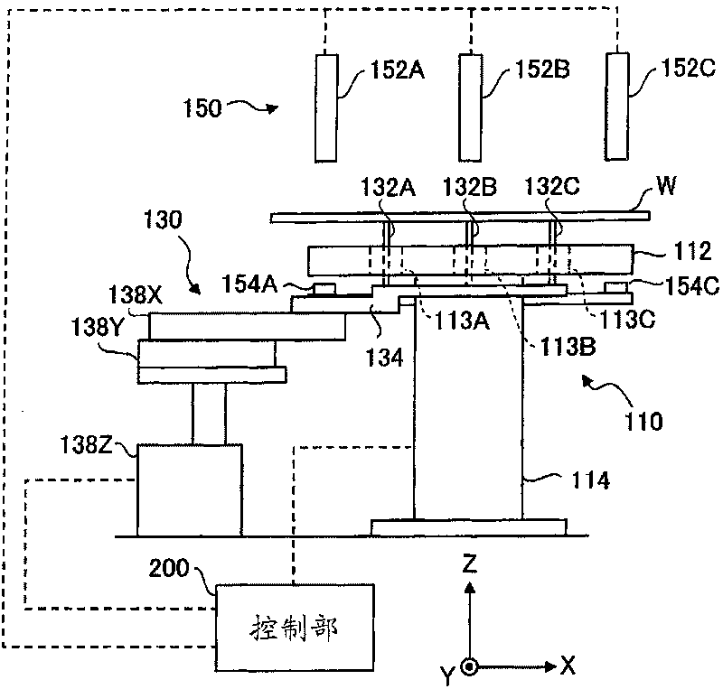
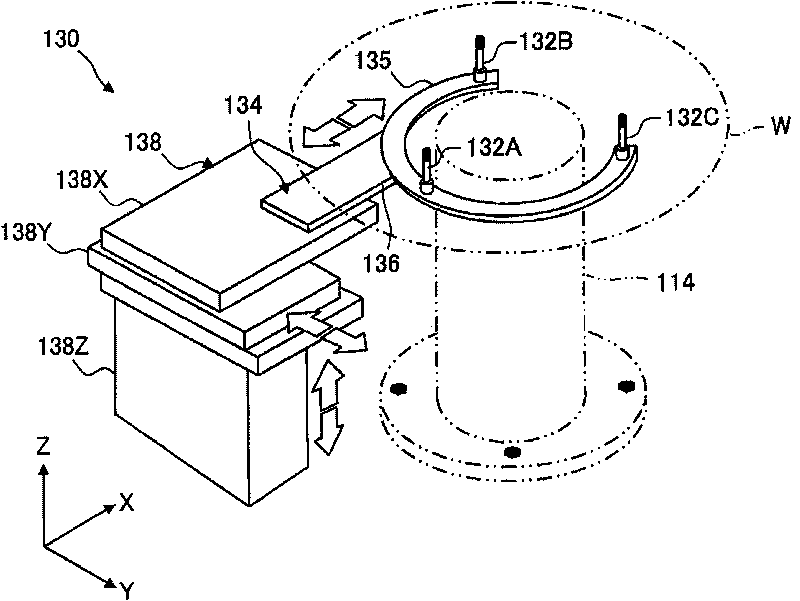
[0062] First, a board transfer device according to an embodiment of the present invention will be described with reference to the drawings. figure 1 It is a perspective view for explaining an installation example of each device, figure 2 yes means figure 1Side views of each device shown. In this embodiment, an embodiment of the substrate transfer device 130 for transferring a substrate such as a semiconductor wafer (hereinafter also simply referred to as “wafer”) W between a transfer arm not shown and the mounting table 112 will be described.
[0063] Such as figure 1 , figure 2 As shown,...
PUM
 Abstract
Description
Claims
Application Information