By-pass circuit and electronic device and display panel using the by-pass circuit
An electronic device and circuit technology, applied to static indicators, instruments, etc., can solve problems such as failure to emit light, failure to effectively improve reliability, failure to operate normally, etc.
- Summary
- Abstract
- Description
- Claims
- Application Information
AI Technical Summary
Problems solved by technology
Method used
Image

Examples
Embodiment Construction
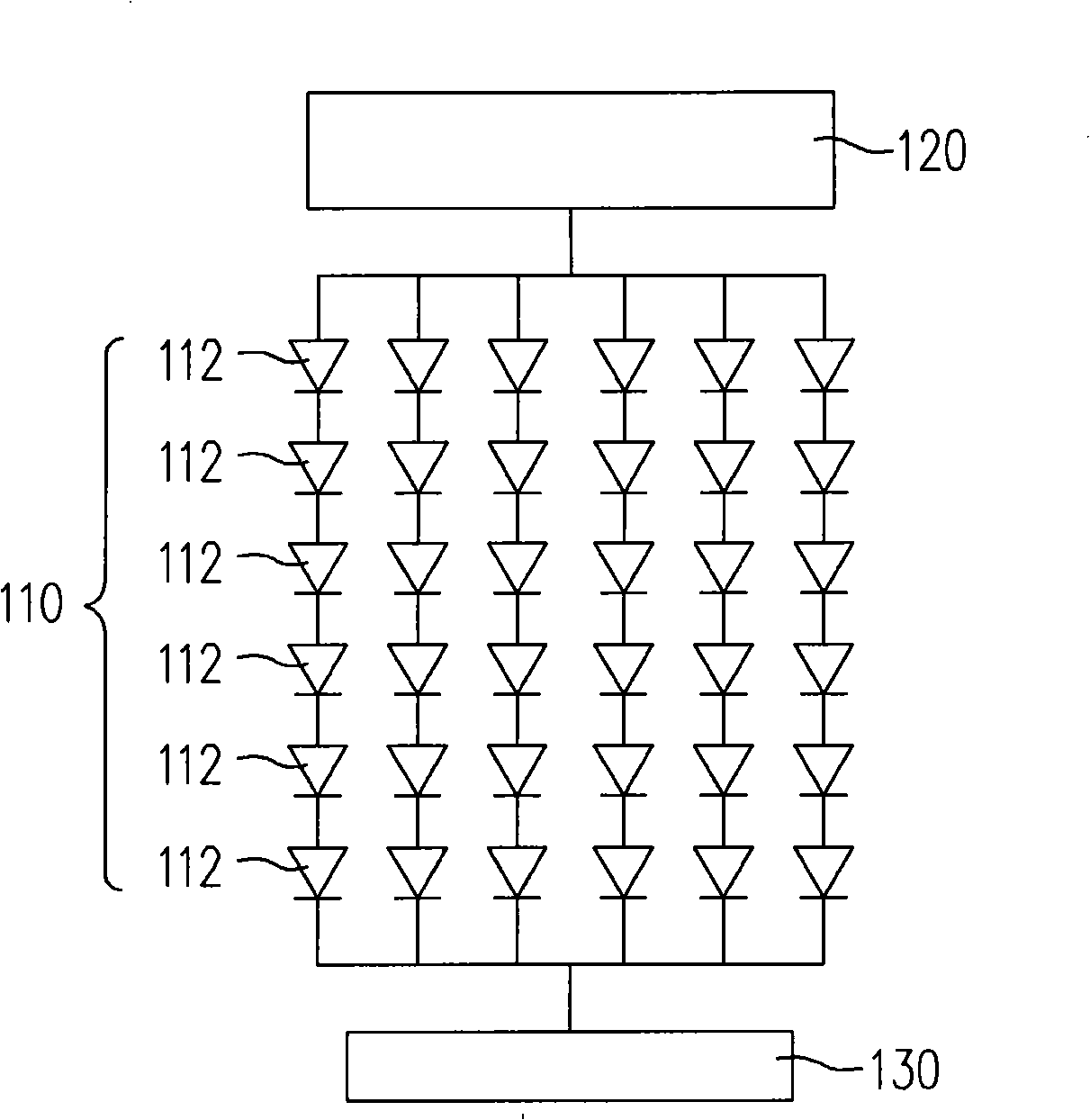
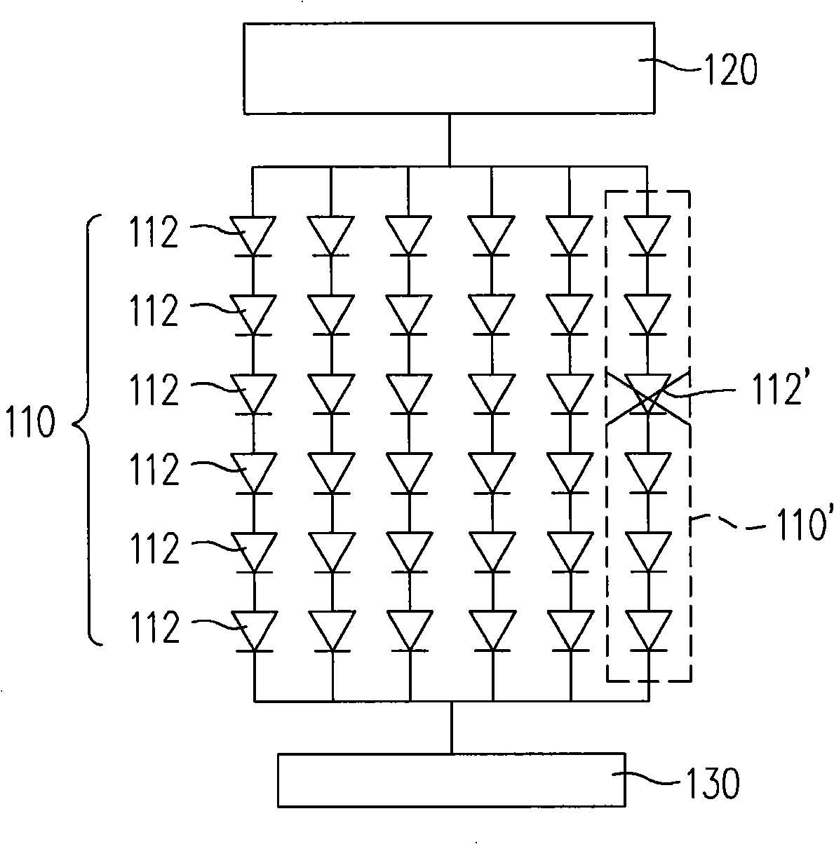
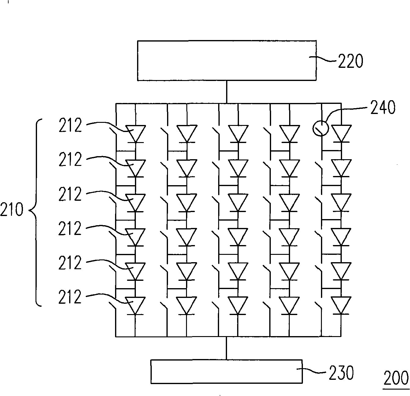
[0022] The bypass line proposed by the present invention mainly includes a thyristor, a first impedance element and a second impedance element. The thyristor is connected in parallel with the electronic element, and the first impedance element and the second impedance element are also connected in parallel with the electronic element after being connected in series. The gate electrode of the thyristor is further coupled between the first impedance element and the second impedance element, wherein the terminal voltage of the electronic component can be divided by the first impedance element and the second impedance element, as the thyristor gate voltage. When an electronic component fails and causes an open circuit, its terminal voltage is the largest, and the gate voltage after voltage division will be greater than the critical voltage of the thyristor, thereby triggering the conduction of the thyristor. In this way, the current that should originally pass through the failed ...
PUM
 Abstract
Description
Claims
Application Information
 - R&D
- Intellectual Property
- Life Sciences
- Materials
- Tech Scout
- Unparalleled Data Quality
- Higher Quality Content
- 60% Fewer Hallucinations
Browse by: Latest US Patents, China's latest patents, Technical Efficacy Thesaurus, Application Domain, Technology Topic, Popular Technical Reports.
© 2025 PatSnap. All rights reserved.Legal|Privacy policy|Modern Slavery Act Transparency Statement|Sitemap|About US| Contact US: help@patsnap.com