Test construction and test method

A technology of test structure and test method, applied in semiconductor/solid-state device test/measurement, electrical components, electric solid-state devices, etc., can solve problems such as EM failure mechanism

Inactive Publication Date: 2009-02-11
UNITED MICROELECTRONICS CORP
View PDF0 Cites 18 Cited by
  • Summary
  • Abstract
  • Description
  • Claims
  • Application Information

AI Technical Summary

Problems solved by technology

However, this kind of wafer-level EM testing is not commonly used in the industry. The main reason is that there are still some controversies that have not been clarified. The first is the failure mechanism of EM. Because the current density applied by EM testing is quite high (for example, 60 to 70 milliamps), its order of magnitude is about ten times that of the traditional PLR-EM test. The researchers suspect that the disconnection mechanism of the metal wire is due to the melting of the aluminum wire due to high temperature (melting), rather than the wafer-level EM we want to measure Phenomenon
Secondly, is there any correlation between the results of wafer-level EM and traditional PLR-EM tests? If the correlation is poor, it is difficult to determine whether the test results of wafer-level EM are correct

Method used


Image

  • Test construction and test method
  • Test construction and test method
  • Test construction and test method

Examples


Embodiment Construction

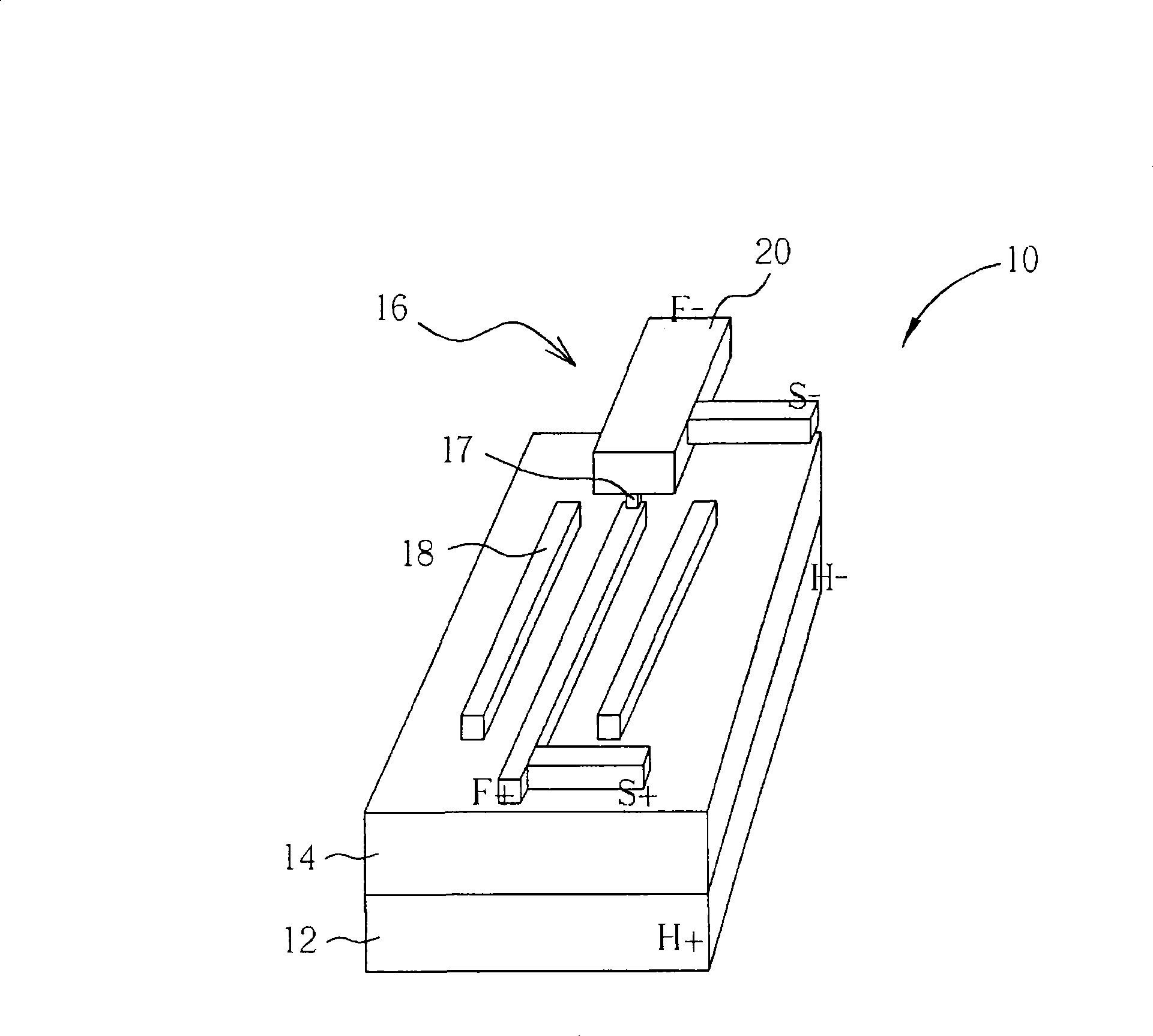
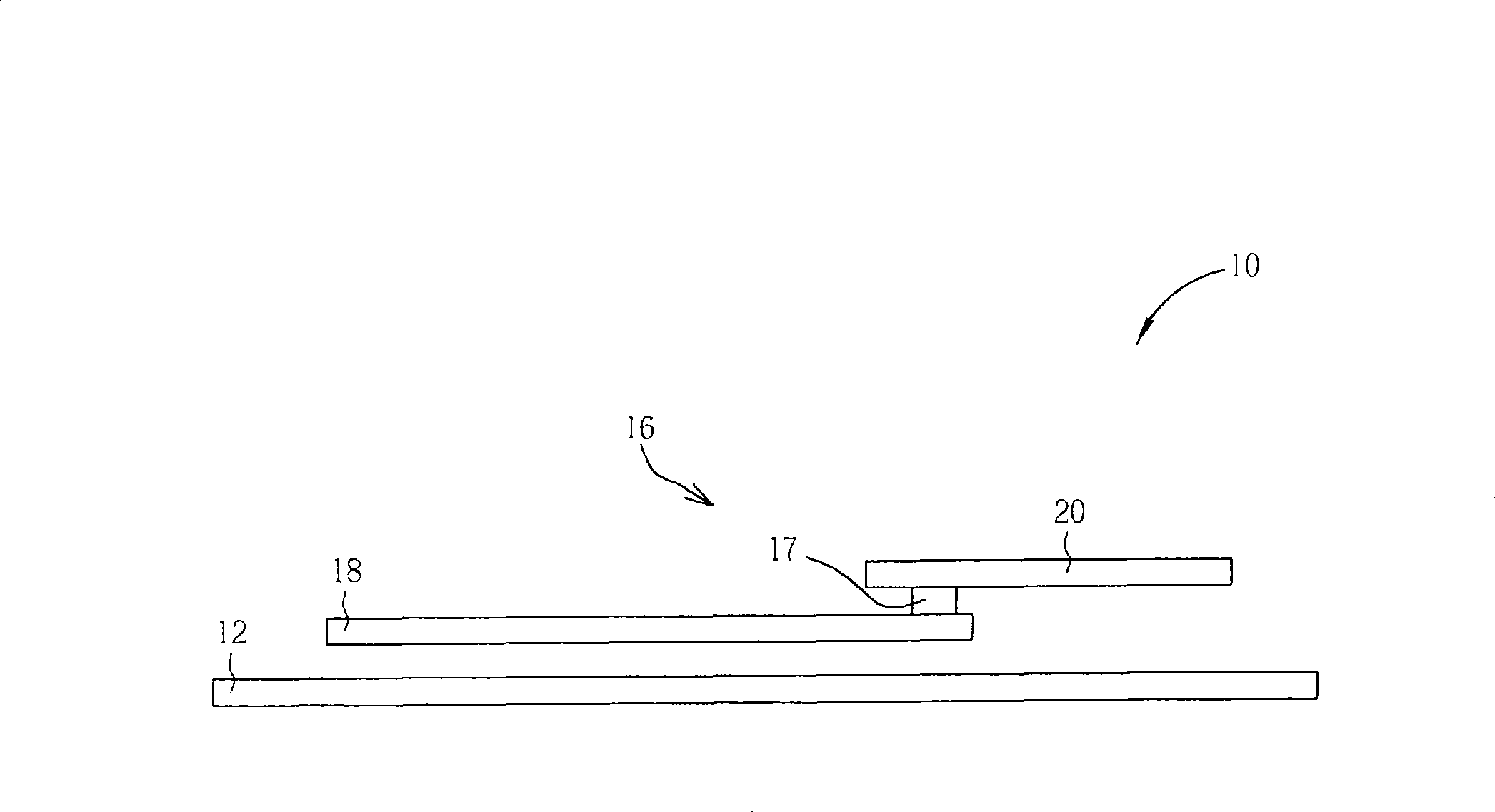
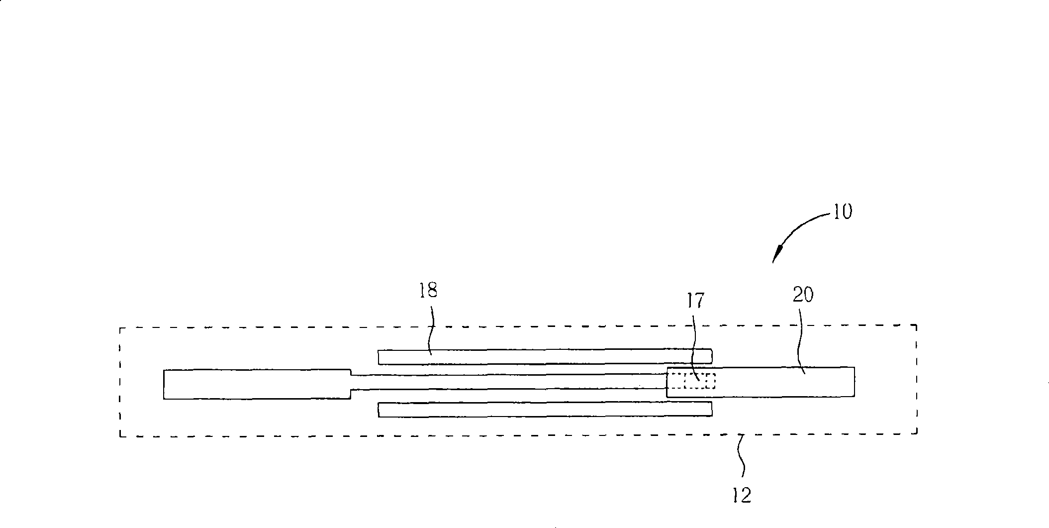
[0030] The test structure according to the invention includes a heating layer and a structure to be tested. The heating layer is located on a wafer and can be connected with electric current for heating. The structure to be tested is located above or adjacent to the heating layer so as to be heated when the heating layer is heated.

[0031] see Figures 1 to 3 , which shows an embodiment of the wafer-level test structure according to the present invention. figure 1 It is a three-dimensional schematic diagram of a wafer-level test structure 10 . figure 2 A schematic cross-sectional view of the test structure 10 at the wafer level is shown. image 3 A schematic top view of the test structure 10 at the wafer level is shown. The test structure 10 according to the present invention can be a wafer-level test structure built on a wafer substrate (not shown). The test structure 10 according to the present invention includes a heating layer 12 and a structure 16 to be tested.

...


PUM


Abstract

The invention discloses a test structure and a test method for a wafer layer, wherein, a heating layer arranged in a wafer is used for directly heating a structure to be tested which is disposed above or beside the heating layer; and after being electrified, the heating layer generates heat. Therefore, the heating of the heating layer and the electric input of the structure to be tested are controlled separately without mutual influence.

Description

technical field [0001] The present invention relates to a test structure and test method, in particular to a test structure and test method for wafer-level reliability test. Background technique [0002] In the manufacturing process of semiconductor devices in semiconductor factories, life test experiments can generally be divided into two categories, which are called "product reliability" and "process reliability" respectively. "Product reliability" testing refers to testing the life cycle of the product in harsh environments such as high temperature, high pressure, and high humidity after the chip is manufactured and initially packaged. And "process reliability" refers to the life test of the semiconductor element material when the initial production of the semiconductor element is completed in the factory, so as to ensure that there is no doubt about the reliability of the product in the subsequent manufacturing process. [0003] The reliability test of the chip factory ...

Claims


Application Information

Patent Timeline
Patent Type & Authority Applications(China)
IPC IPC(8): H01L23/00H01L23/544H01L21/66
Inventor 柯文雄张文俊苏冠丞
Owner UNITED MICROELECTRONICS CORP
Why Eureka
Try Eureka