Semiconductor packaging construction with weld crack restraint ring

A semiconductor and structural technology, applied in the field of high-density packaging stacking module architecture, can solve the problems of stress resistance becoming more sensitive, general products do not have suitable structure, open circuit, etc., to increase the welding fixing strength and high product durability. degree, and the effect of inhibiting the spread of cracks

Inactive Publication Date: 2009-02-18
POWERTECH TECHNOLOGY
View PDF2 Cites 7 Cited by
  • Summary
  • Abstract
  • Description
  • Claims
  • Application Information

AI Technical Summary

Problems solved by technology

[0005] However, it becomes more sensitive to stress resistance. When stress is generated at the soldering interface of the stud bumps 130, cracks will propagate along the inclined continuous sidewalls 131 of the stud bumps 130, resulting in electrical failure. open circuit
[0006] It can be seen that the above-mentioned existing semiconductor packaging structure obviously still has inconvenience and defects in structure and use, and needs to be further improved urgently.
In order to solve the above-mentioned problems, the relevant manufacturers have tried their best to find a solution, but for a long time no suitable design has been developed, and the general product has no suitable structure to solve the above-mentioned problems. This is obviously the relevant industry. Urgent problem

Method used


Image

  • Semiconductor packaging construction with weld crack restraint ring
  • Semiconductor packaging construction with weld crack restraint ring
  • Semiconductor packaging construction with weld crack restraint ring

Examples


no. 1 Embodiment

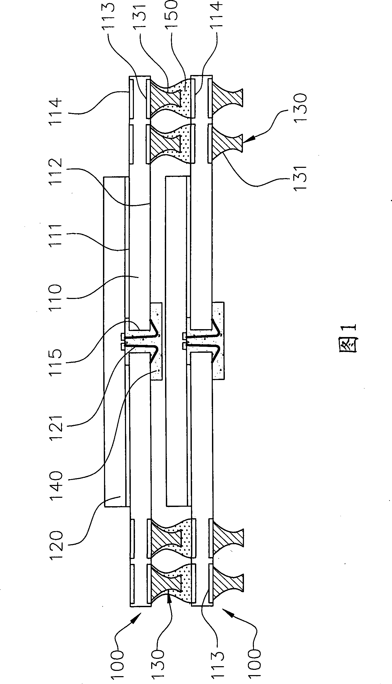
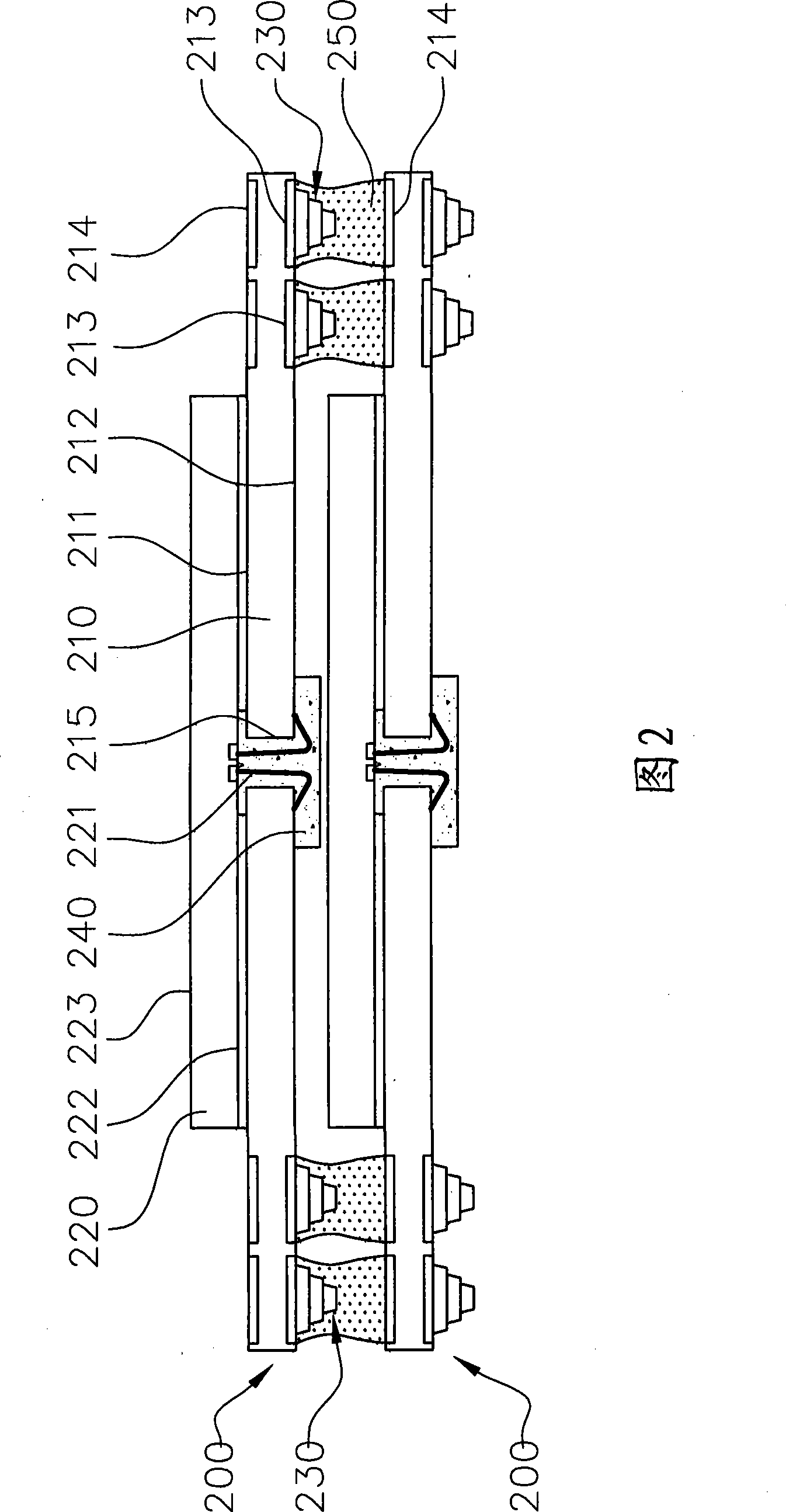
[0069] Please refer to FIG. 2 , which is a schematic cross-sectional view of stacked semiconductor package structures with solder crack suppression rings according to the first embodiment of the present invention. It is a stacking combination of two semiconductor package structures 200 , but without limitation, more semiconductor package structures 200 can be stacked on top, such as three, four or more. Each semiconductor package structure 200 mainly includes a chip carrier 210 , a chip 220 and a plurality of tower bumps 230 .

[0070] The chip carrier 210 mentioned above can be a multi-layer printed circuit board with a double-sided electrical conduction structure. The wafer carrier 210 has an upper surface 211 and a lower surface 212, wherein:

[0071] The lower surface 212 is provided with a plurality of first conductive pads 213 , which can be used as external pads of the chip carrier 210 . In this embodiment, the semiconductor package structure 200 is suitable for packa...

no. 2 Embodiment

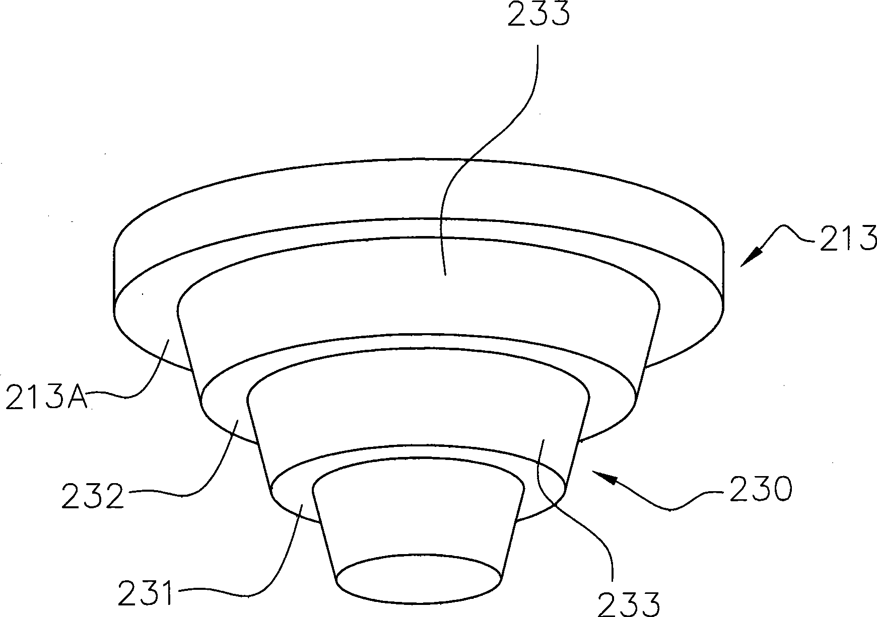
[0086] see Figure 5 Shown is a schematic perspective view of another tower-shaped bump shape of the semiconductor package structure according to the second embodiment of the present invention. The other shape of the tower-shaped protrusion is to replace the tower-shaped protrusions 330 with another tower-shaped protrusion 330A with a change in shape. The tower-shaped protrusion 330A is composed of multi-segmented cones. There is a first crack suppression ring 331A and at least one second crack suppression ring 332A. Wherein, the first crack suppression ring 331A and the second crack suppression ring 332A are roughly parallel to the first conductive pads 313 to suppress the diffusion of welding cracks. The second crack suppression ring 332A is located between the first crack suppression ring 331A and the corresponding first contact pad 313 , and is parallel to but not coplanar with the first crack suppression ring 331A. In this embodiment, the inner diameter of the second cr...


PUM


Abstract

The invention is related to a semiconductor encapsulating structure, comprising: a wafer carrier that includes an upper surface and a lower surface, wherein the lower surface is provided with plural first conduction pads; a water which is arranged and electrically connected with the wafer carrier; and plural turriform projections that are correspondingly arranged on these first conduction pads, for welding outwards, each of the turriform projections includes at least a first crack suppression ring which is parallel to these first conduction pads and which is used for suppressing expansion of the welding crack. The invention can effectively prevent the expansion of crack at solder-welding interfaces and avoid the issue of electric breaking as the external terminals provided at the wafer carrier are the turriform projections and at least one crack suppression ring is contained in the invention. Furthermore, the invention also can increase welding fixation strength in order to achieve high production durability. The invention is particularly suitable for a stacked structure and extremely practicable owing to effective suppression of the crack expansion at micro-contact welding sites.

Description

technical field [0001] The invention relates to a three-dimensional stacking technology of a semiconductor package structure, in particular to a semiconductor package structure with a welding crack suppression ring, which can be applied to a package-on-package module (POP) structure of a high-density package stack. Background technique [0002] With the development trend of miniaturization of electronic products, the area available for setting semiconductor packaging structures on the surface of the printed circuit board is getting smaller and smaller. Therefore, there is a three-dimensional stacking technology for semiconductor packaging structures, which is to stack a plurality of semiconductor packaging structures together to form a Package-On-Package module (POP), in order to meet the small surface bonding area and high-density components. set requirements. However, soldering defects are a major problem during the bonding process of the package stack. The fine pitch of ...

Claims


Application Information

Patent Timeline
Patent Type & Authority Applications(China)
IPC IPC(8): H01L23/00H01L23/488
CPCH01L2924/0002H01L2224/73215H01L2224/32225H01L2224/4824
Inventor 范文正
Owner POWERTECH TECHNOLOGY
Why Eureka
Try Eureka