Method and system for high power switching
A technology of field effect transistors and gates, which is applied in the field of signal processing, and can solve problems such as high cost, increased switch insertion loss, and large circuit size
- Summary
- Abstract
- Description
- Claims
- Application Information
AI Technical Summary
Problems solved by technology
Method used
Image

Examples
Embodiment Construction
[0011] By referring to Figure 1 of the accompanying drawings to Figure 3B , to better understand the exemplary embodiments of the present invention and advantages thereof, like reference numerals are used in the various drawings to indicate like and corresponding parts.
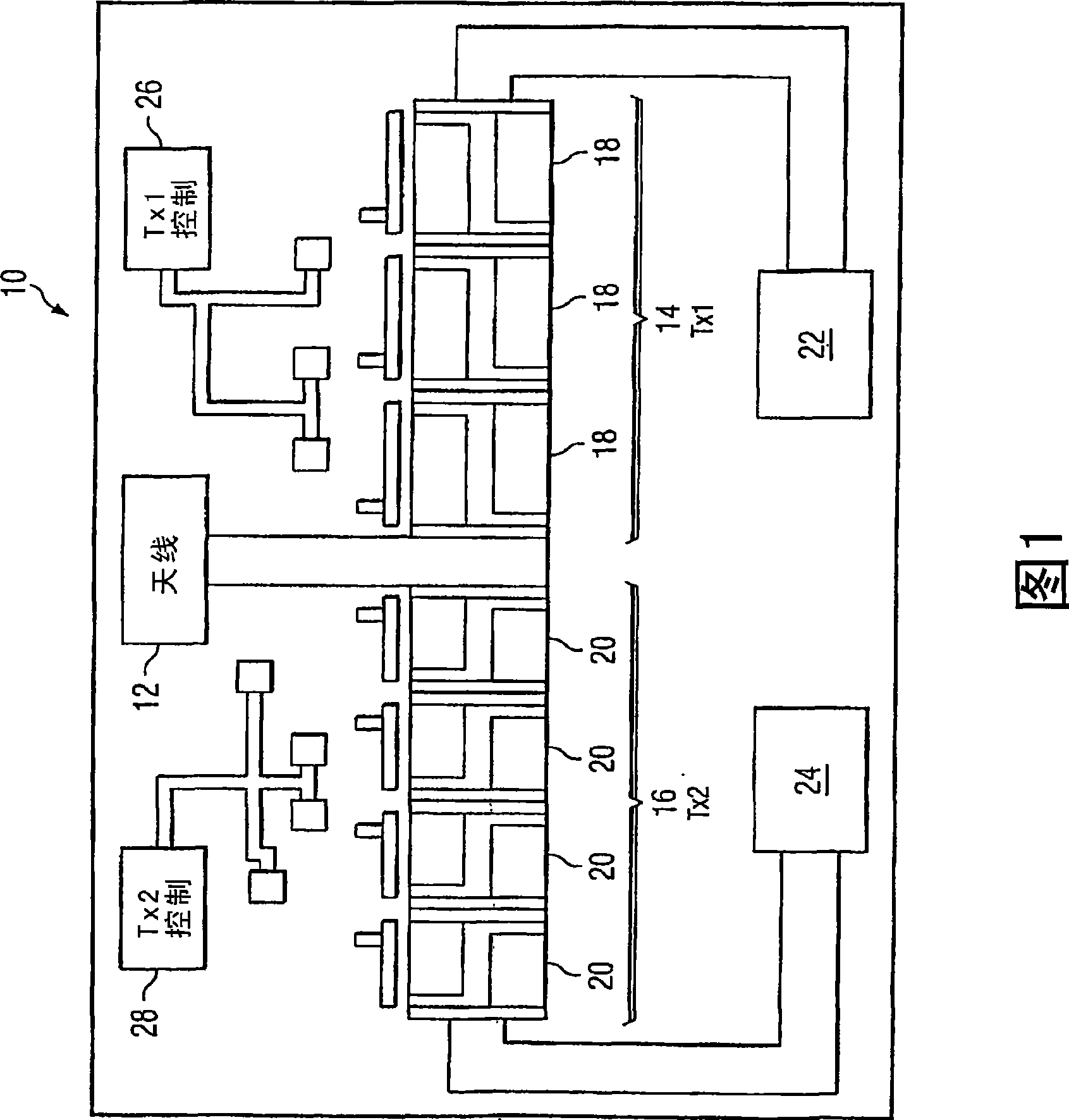
[0012] FIG. 1 is a schematic diagram illustrating a conventional high power switch 10 . Switch 10 includes antenna node 12 , first leg 14 , second leg 16 , and output nodes 22 and 24 . The first leg 14 includes a plurality of field effect transistors (FETs) 18 stacked in series. The second leg 16 includes a plurality of FETs 20 stacked in series.
[0013] In operation, a radio frequency or alternating current signal is received by antenna 12 and the received signal is switched to either output 22 or output 24 . This switching is accomplished by either all FETs 18 or all FETs 20 on the respective paths 14 and 16 being on or off together. In certain implementations, such as cellular telephones, the control...
PUM
 Abstract
Description
Claims
Application Information
 - R&D
- Intellectual Property
- Life Sciences
- Materials
- Tech Scout
- Unparalleled Data Quality
- Higher Quality Content
- 60% Fewer Hallucinations
Browse by: Latest US Patents, China's latest patents, Technical Efficacy Thesaurus, Application Domain, Technology Topic, Popular Technical Reports.
© 2025 PatSnap. All rights reserved.Legal|Privacy policy|Modern Slavery Act Transparency Statement|Sitemap|About US| Contact US: help@patsnap.com