FFS type TFT-LCD array substrate structure and manufacturing method thereof

A technology of array substrate structure and manufacturing method, which is applied in semiconductor/solid-state device manufacturing, photoengraving process of pattern surface, instruments, etc., and can solve problems such as yield reduction, gate line-transparent electrode short circuit, quality problems, etc.

Active Publication Date: 2009-02-25
K TRONICS (SUZHOU) TECH CO LTD +1
View PDF0 Cites 20 Cited by
  • Summary
  • Abstract
  • Description
  • Claims
  • Application Information

AI Technical Summary

Problems solved by technology

Remaining grid lines will lead to grid line-transparent electrode short circuit problems, and residual transparent electrodes will cause defective pixels, which not only becomes a very serious quality problem, but also greatly affects the production of array substrates, resulting in a decrease in yield

Method used


Image

  • FFS type TFT-LCD array substrate structure and manufacturing method thereof
  • FFS type TFT-LCD array substrate structure and manufacturing method thereof
  • FFS type TFT-LCD array substrate structure and manufacturing method thereof

Examples


Embodiment Construction

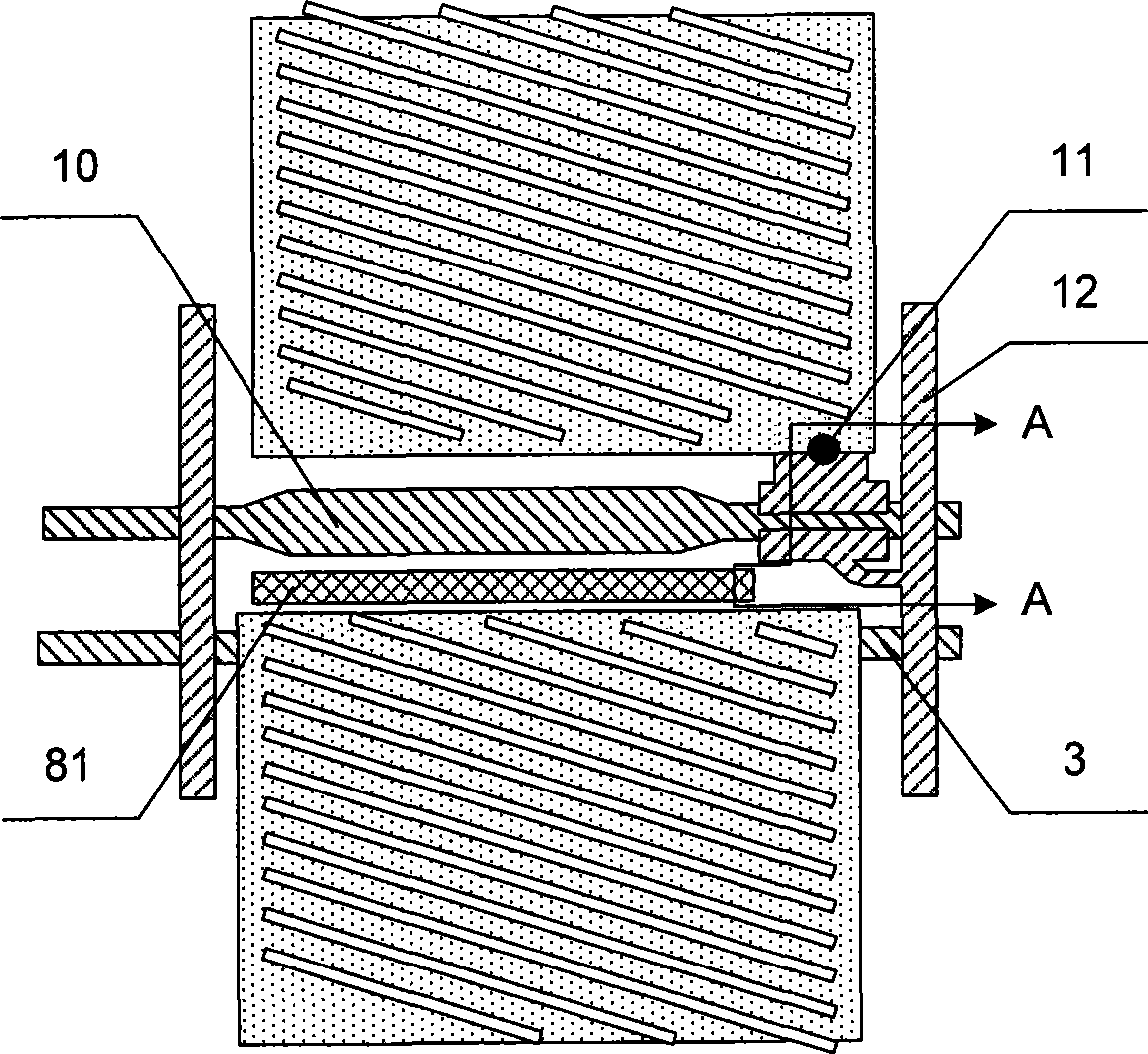
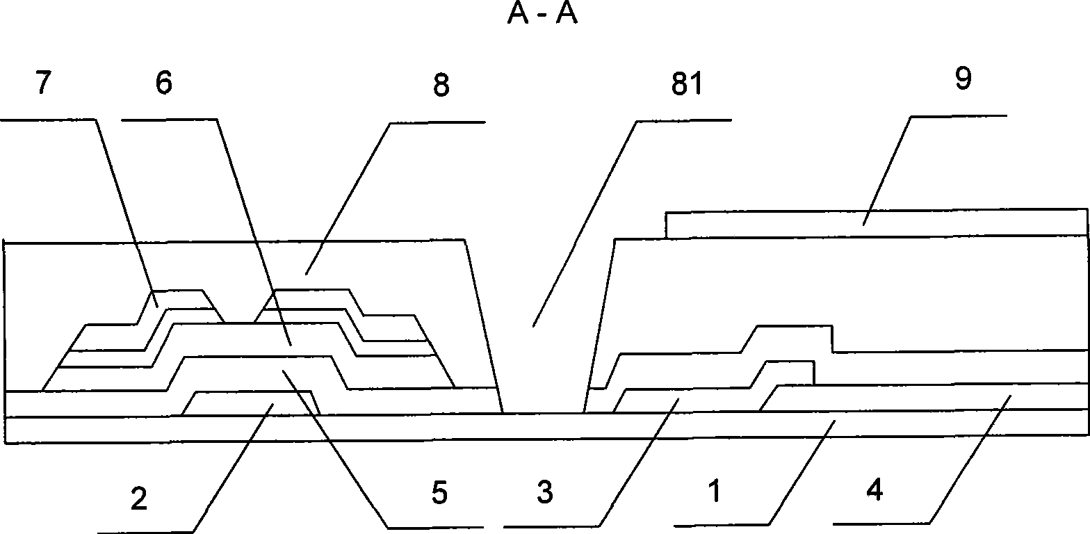
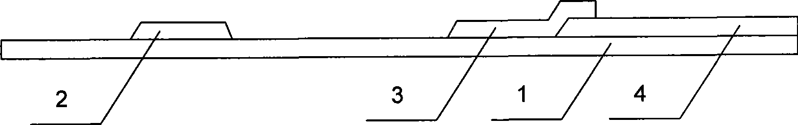
[0037] figure 1 It is a schematic diagram of the structure of the FFS type TFT-LCD array substrate of the present invention, figure 2 for figure 1 Middle A-A sectional view. like figure 1 , figure 2 As shown, the array substrate structure of the present invention includes a glass substrate 1, and gate electrodes 2, gate lines 10, common electrode lines 3 and transparent electrodes 4 are formed on the glass substrate, and the gate lines 10 and common electrode lines 3 are arranged in isolation. It is connected with the transparent electrode 4 to form a common electrode. The gate insulating layer 5 is formed on the glass substrate and covers the gate electrode 2, the gate line 10, the common electrode line 3 and the transparent electrode 4. The active layer 6 and the source-drain electrode layer 7 are sequentially formed on the On the glass substrate and above the gate electrode 2, the source-drain electrode layer 7 includes the source electrode, the drain electrode and th...


PUM

PropertyMeasurementUnit
widthaaaaaaaaaa
widthaaaaaaaaaa
thicknessaaaaaaaaaa

Abstract

The invention relates to an FFS-type TFT-LCD array base plate structure and a manufacturing method thereof. The array base plate structure includes a glass base plate, a grid electrode formed on the glass base plate, a grid line, a common electrode line and a transparent electrode, a grid insulating layer formed on the glass base plate, an active layer and a source-drain electrode layer sequentially formed on the glass base plate and arranged above the grid electrode, a passivation layer formed on the glass base plate, a via hole formed on the passivation layer, a blocking channel formed on the passivation layer and used for blocking off the grid line and the common electrode line, and a pixel electrode formed on the passivation layer and connected with the drain electrode in the source-drain electrode layer through the via hole. Through adding the blocking channel into the arranged base plate, the invention can efficiently repair the badness caused by the grid line residual and the common electrode residual. The invention introduces the repair concept into the process of designing a mask plate, and has good effect on repairing the badness caused by the grid line residual and the common electrode residual, etc.

Description

technical field [0001] The invention relates to a thin film transistor liquid crystal display and a manufacturing method thereof, in particular to an FFS type TFT-LCD array substrate structure and a manufacturing method thereof. Background technique [0002] Thin Film Transistor Liquid Crystal Display (TFT-LCD for short) has the characteristics of small size, low power consumption, and no radiation, and occupies a dominant position in the current flat panel display market. Fringe Field Switching (FFS for short) generates a fringe electric field through the electrodes between pixels in the same plane, so that the aligned liquid crystal molecules between the electrodes and directly above the electrodes can be rotated in the direction of the plane (parallel to the substrate). The light transmission efficiency of the liquid crystal layer is improved while the viewing angle is large. [0003] The prior art FFS type TFT-LCD array substrate structure includes a glass substrate, a ...

Claims


Application Information

Patent Timeline
Patent Type & Authority Applications(China)
IPC IPC(8): G02F1/1362G03F7/00H01L21/027
Inventor 吕敬崔承镇
Owner K TRONICS (SUZHOU) TECH CO LTD
Why Eureka
Try Eureka