Array substrate and repair method thereof

A repair method and array substrate technology, applied in the direction of electrical components, electric solid devices, circuits, etc., can solve problems such as repair failure, and achieve the effect of improving product yield and product quality, and repairing bad points

Active Publication Date: 2018-08-14
TCL CHINA STAR OPTOELECTRONICS TECH CO LTD
View PDF3 Cites 0 Cited by
  • Summary
  • Abstract
  • Description
  • Claims
  • Application Information

AI Technical Summary

Problems solved by technology

[0006] In the prior art, there is another method for repairing the spot defects caused by abnormal via holes, that is, through the via hole 61 by laser, so that the pixel electrode 70 and the drain electrode 502 are welded together; however, due to the via hole 61 There are two layers of metal below, which are the drain electrode 502 in the first metal layer 2 and the storage capacitor electrode 204 in the second metal layer 5, so it is easy to connect the drain electrode 502 and the storage capacitor electrode 204 in the laser laser process. welded together, causing the repair to fail

Method used


Image

  • Array substrate and repair method thereof
  • Array substrate and repair method thereof
  • Array substrate and repair method thereof

Examples


Embodiment Construction

[0037] In order to further illustrate the technical means adopted by the present invention and its effects, the following describes in detail in conjunction with preferred embodiments of the present invention and accompanying drawings.

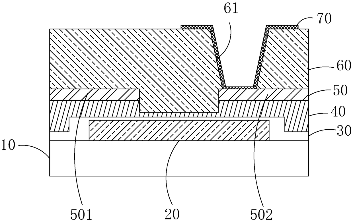
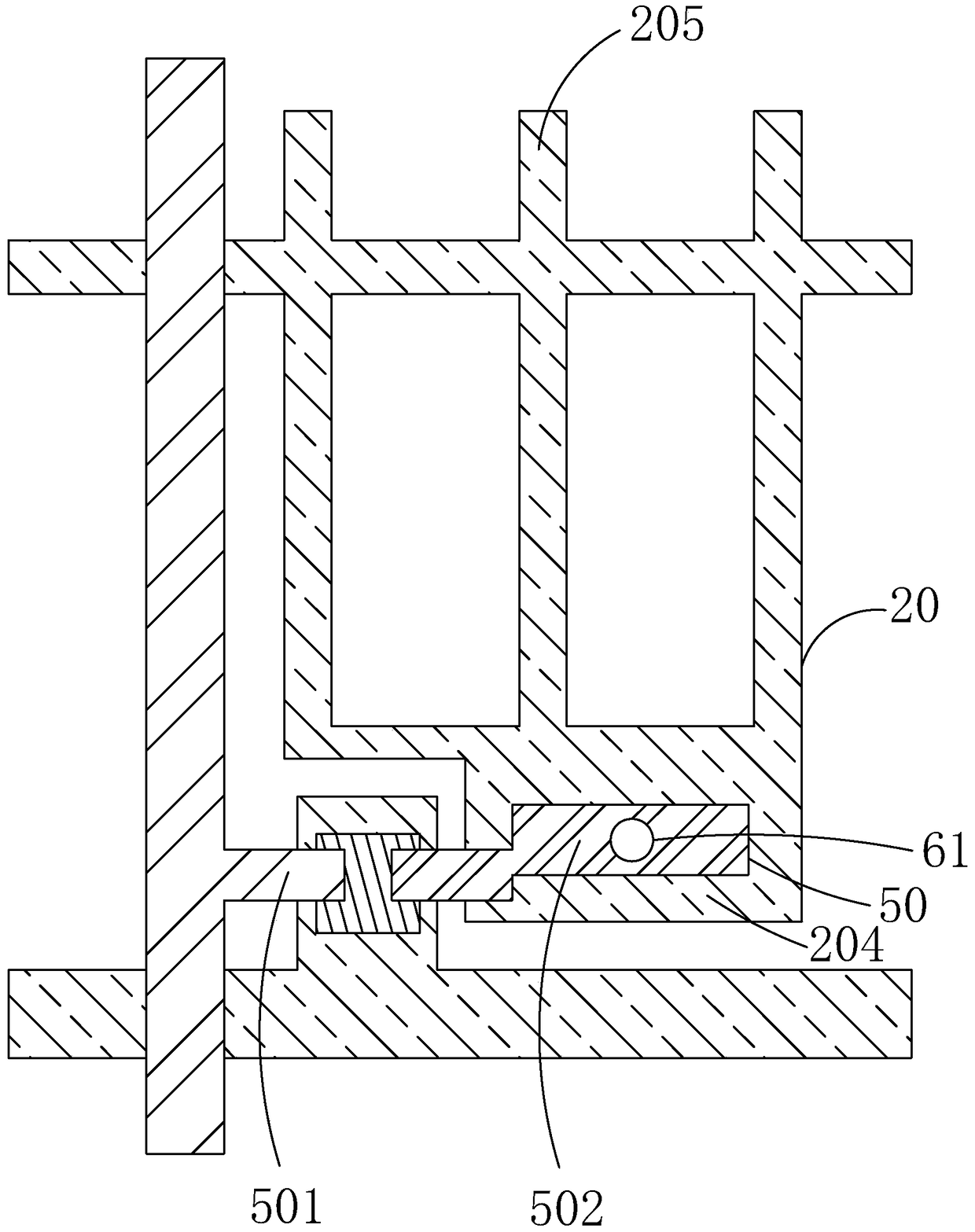
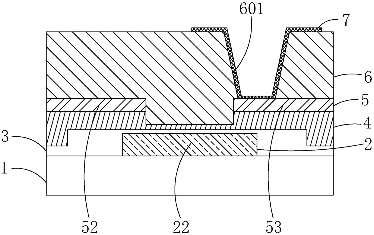
[0038] see image 3 and Figure 4 , the present invention provides an array substrate, comprising: a base substrate 1, a first metal layer 2 disposed on the base substrate 1, an insulating layer 3 disposed on the first metal layer 2, an insulating layer 3 disposed on the insulating The semiconductor layer 4 on the layer 3, the second metal layer 5 on the semiconductor layer 4, the organic material layer 6 on the second metal layer 5, and the pixel electrode layer 7 on the organic material layer 6 ;

[0039]The first metal layer 2 includes a scan line 21, a gate 22 connected to the scan line 21, a storage capacitor electrode 24 spaced apart from the gate 22, and a common electrode line 25 connected to the storage capacitor electrode 24;

[0...


PUM


Abstract

The invention provides an array substrate and a repair method thereof. According to the method, a storage capacitor electrode in a first metal layer and a drain in a second metal layer are arranged in a staggered manner; one part of a through hole in an organic material layer is corresponding to a region on the drain, wherein the region on the drain is overlapped with the storage capacitor electrode; the other part of the through hole in the organic material layer is corresponding to a region on the drain, wherein the region on the drain is not overlapped with the storage capacitor electrode; when anomalies occur on the through hole, and a pixel electrode layer and the drain cannot contact with each other effectively, and laser can be adopted to perform laser processing on the part of the through hole which is corresponding to the region on the drain which is not overlapped with the storage capacitor electrode, and therefore, the pixel electrode layer and the drain can be weld together; and at a laser welding spot site, the first metal layer is arranged below the drain, and therefore, the first metal layer and the second metal layer will not be welded together. With the array substrate and the repair method thereof adopted, malfunction of spots caused by the anomalies of the through hole can be repaired, and dark spots can be converted to bright spots, and the yield and quality of products can be improved.

Description

technical field [0001] The present invention relates to the field of display technology, in particular to an array substrate and a repair method thereof. Background technique [0002] A liquid crystal display (LCD, Liquid Crystal Display) has many advantages such as a thin body, power saving, and no radiation, and has been widely used. Such as: LCD TV, mobile phone, personal digital assistant (PDA), digital camera, computer screen or laptop screen, etc. [0003] Generally, a liquid crystal display device includes a housing, a liquid crystal display panel disposed in the housing, and a backlight module disposed in the housing. Among them, the structure of the liquid crystal display panel is mainly composed of an array substrate (Thin FilmTransistor Array Substrate, TFT Array Substrate), a color filter substrate (Color Filter Substrate, CF Substrate), and a liquid crystal layer (Liquid Crystal Layer) arranged between the two substrates. Its working principle is to control th...

Claims


Application Information

Patent Timeline
Patent Type & Authority Patents(China)
IPC IPC(8): H01L27/12H01L21/77
CPCH01L27/124H01L27/1244H01L27/1259
Inventor 姜祥卫
Owner TCL CHINA STAR OPTOELECTRONICS TECH CO LTD
Why Eureka
Try Eureka