Array substrate, repairing method thereof and display device

A technology of array substrates and thin film transistors, applied in the fields of instruments, nonlinear optics, optics, etc., can solve the problems of unfavorable high-resolution TFT-LCD, reduced picture display effect, complicated production process, etc., so as to improve the picture display effect and avoid Dark point processing, to achieve the effect of resolution

Active Publication Date: 2018-09-28
BOE TECH GRP CO LTD +1
View PDF5 Cites 5 Cited by
  • Summary
  • Abstract
  • Description
  • Claims
  • Application Information

AI Technical Summary

Problems solved by technology

[0004] In the production process of the array substrate, due to the complex production process, affected by the production process and the factory environment, it may cause foreign matter or film breakage in the pixel unit to cause a short circuit, which will appear on the display screen and be easier for human eyes to identify Display defects that seriously affect the display quality of the screen
Existing repairing technologies usually perform simple repairing by performing dark-spot processing on abnormally displayed pixel units, which will reduce the display effect of the screen and is not conducive to the realization of high-resolution TFT-LCD

Method used


Image

  • Array substrate, repairing method thereof and display device
  • Array substrate, repairing method thereof and display device
  • Array substrate, repairing method thereof and display device

Examples


Embodiment 1

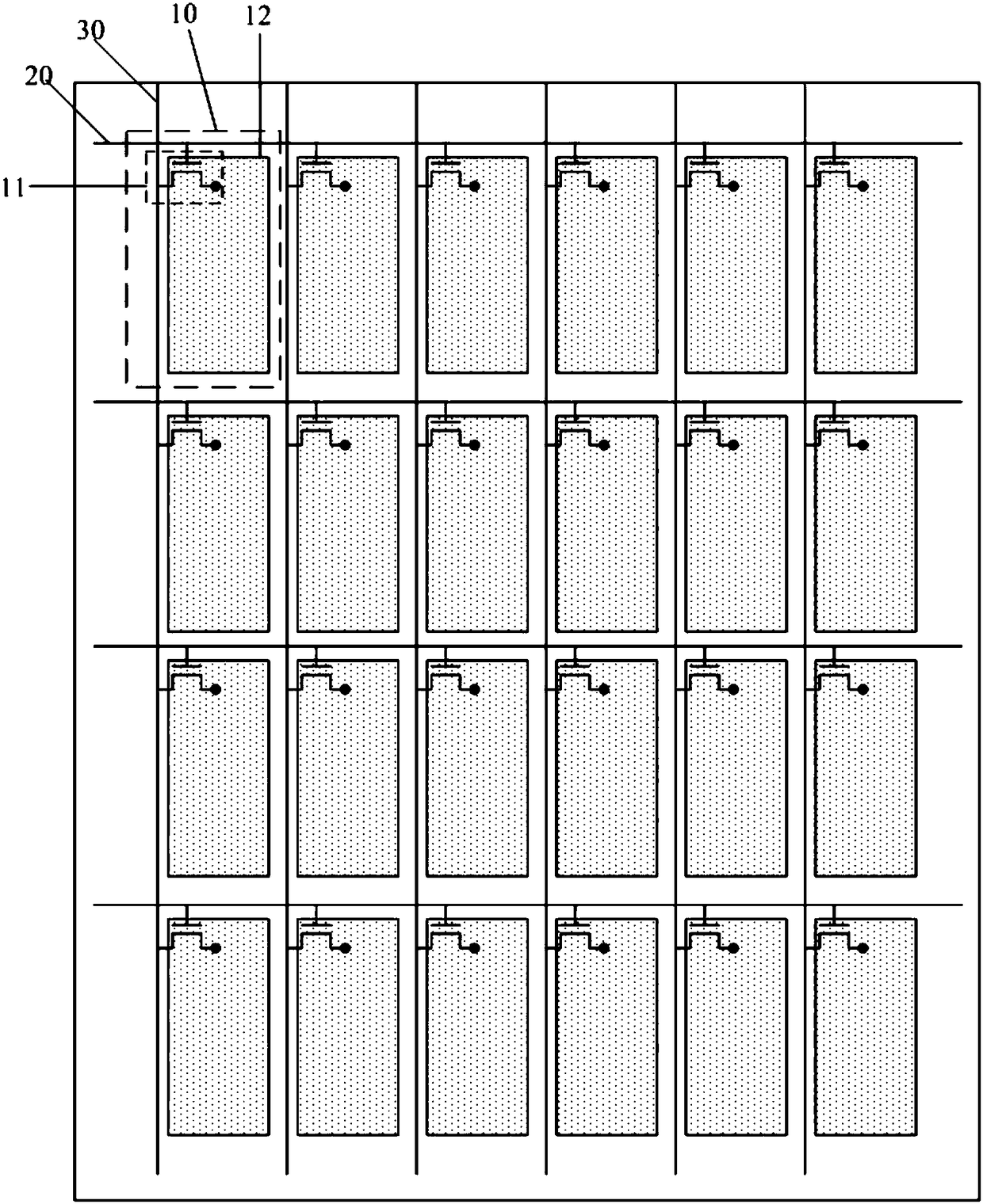
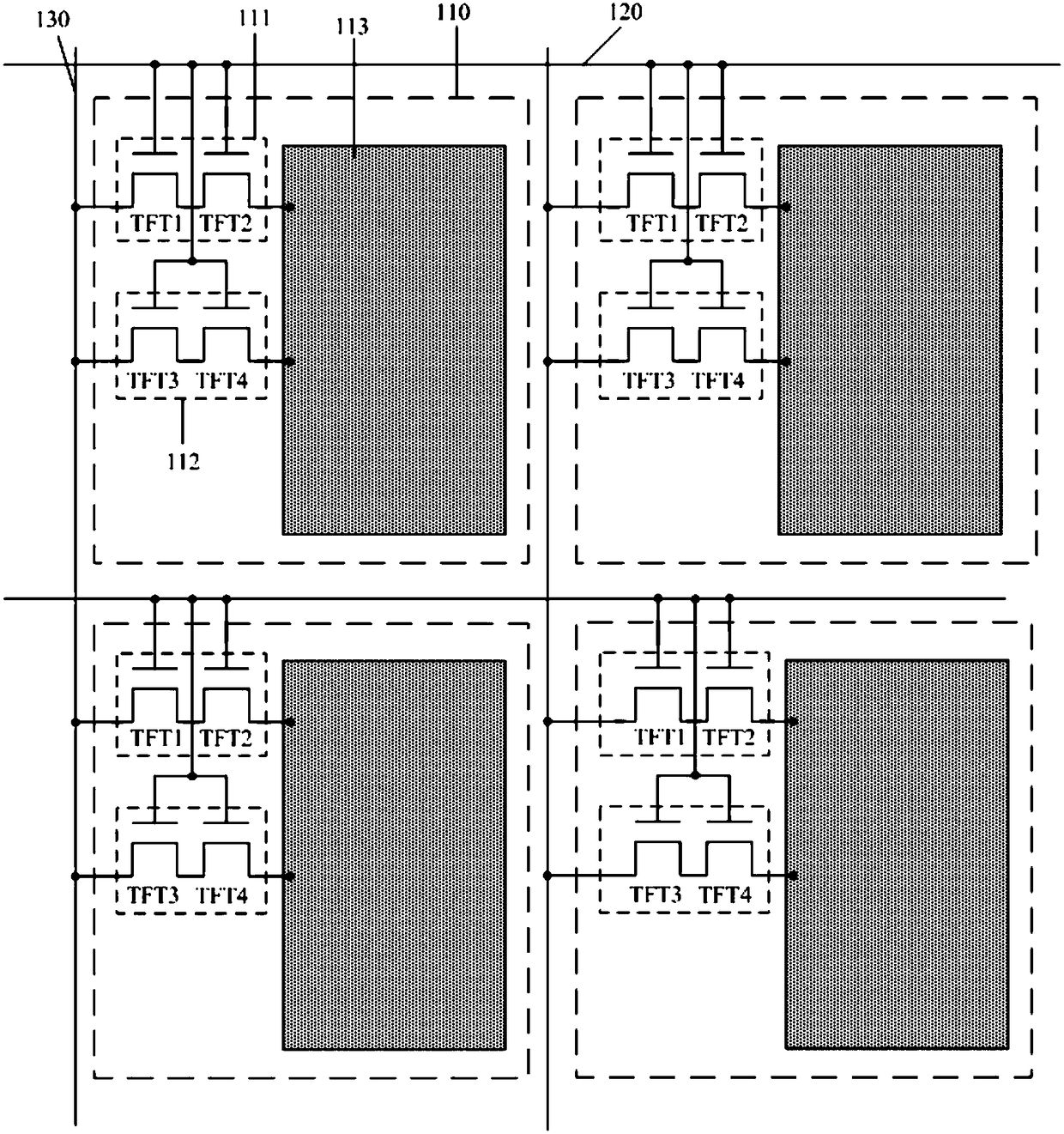
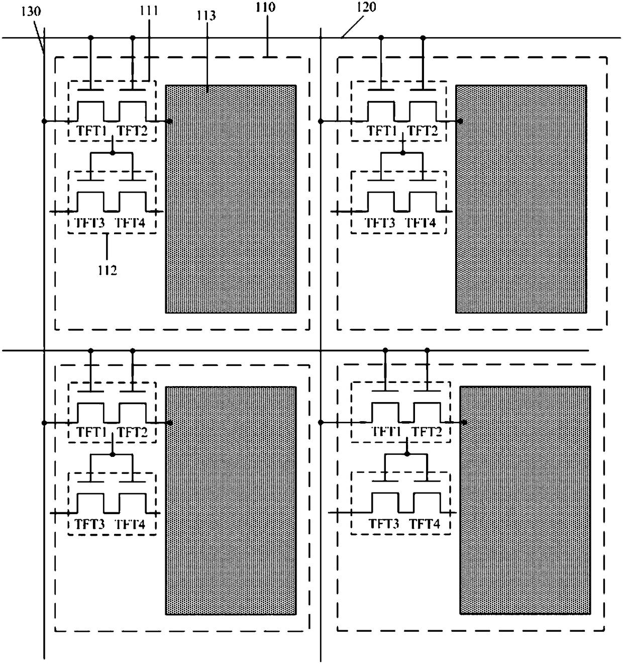
[0050] In specific implementation, such as Figure 2a As shown, the array substrate may further include: a plurality of gate lines 120 and a plurality of data lines 130: in the embodiment of the present invention, the pixel unit 110 further includes a pixel electrode 113; wherein, in the same pixel unit 110, the repair thin film transistor 112 The gate of the switching thin film transistor 111 is electrically connected to the same gate line 120, the source of the repairing thin film transistor 112 and the source of the switching thin film transistor 111 are both electrically connected to the same data line 130, and the repairing thin film transistor 112 The drain of the switching thin film transistor 111 and the drain of the switching thin film transistor 111 are both electrically connected to the pixel electrode 113 . In this way, under the control of the switching scanning signal transmitted by the gate line 120, the switching thin film transistor 111 and the repairing thin ...

Embodiment 2

[0064] In order to reduce power consumption, at least one electrode among the gate, source and drain of the repaired thin film transistor may also be in a floating state during specific implementation. That is, repairing at least one electrode among the gate, source and drain of the thin film transistor is not electrically connected to the corresponding signal line and pixel electrode. In this way, when it is detected that the switching thin film transistor in the pixel unit does not have defects such as a short circuit caused by foreign objects, only the switching thin film transistor is used to transmit signals, so as to reduce power consumption. When it is detected that the switching thin film transistor in the pixel unit has defects such as a short circuit due to foreign matter, the repairing thin film transistor is welded to a corresponding position of the signal line to replace the switching thin film transistor to work. In specific implementation, the structure of the r...


PUM


Abstract

The invention discloses an array substrate, a repairing method thereof and a display device. In case of defects of switching thin film transistors in pixel units, repairing thin film transistors are arranged in the pixel units in the embodiment for repairing the pixel units to replace the switching thin film transistors with defects to work. The repairing thin film transistors can repair the defects, so that darkening of the pixel units can be avoided, the picture display effect is improved, and a high-resolution display panel is achieved.

Description

technical field [0001] The invention relates to the field of display technology, in particular to an array substrate, its repair method and a display device. Background technique [0002] At present, thin film transistor liquid crystal display panel (Thin Film Transistor Liquid Crystal Display, referred to as TFT-LCD) has become the mainstream of flat panel display, and has been widely used in televisions, mobile phones, computers and other fields. TFT-LCD generally includes: an array substrate and a counter substrate arranged oppositely, and a liquid crystal layer filled between the two substrates. Its working principle is to control the rotation of liquid crystal molecules in the liquid crystal layer by applying a driving voltage to the liquid crystal layer, and refract the light from the backlight module to generate a picture. [0003] Such as figure 1 As shown, the array substrate of the existing TFT-LCD generally includes a plurality of pixel units 10 arranged in an a...

Claims


Application Information

Patent Timeline
Patent Type & Authority Applications(China)
IPC IPC(8): G02F1/1362G02F1/1368
CPCG02F1/13624G02F1/136259G02F1/136286G02F1/1368G02F1/136268
Inventor 刘振定南春香曹丽丽潘晓东胡志明朱彦荣麻小川袁亮
Owner BOE TECH GRP CO LTD
Why Eureka
Try Eureka