Automatic optical detection device and method

An automatic optical inspection and light technology, which is applied in the direction of using optical devices, measuring devices, optical testing defects/defects, etc., can solve the problems of slow inspection speed, production efficiency and data processing speed

Inactive Publication Date: 2009-03-11
AJUHITEK
View PDF0 Cites 10 Cited by
  • Summary
  • Abstract
  • Description
  • Claims
  • Application Information

AI Technical Summary

Problems solved by technology

[0004] In order to inspect one surface in this way, if the upper illuminator and the lower illuminator are used to acquire images separately for inspection, the inspection speed will be slowed down, and various problems will arise due to the decrease in productivity and data processing speed

Method used


Image

  • Automatic optical detection device and method
  • Automatic optical detection device and method
  • Automatic optical detection device and method

Examples


Embodiment Construction

[0022] Various modifications can be made to the embodiment of the present invention, and the scope of the present invention is not interpreted as being limited to the embodiment described below. This embodiment is provided only for the purpose of more completely explaining the invention to those skilled in the art. Therefore, the shapes and the like of elements in the drawings are exaggerated for clearer illustration.

[0023] The following will refer to the attached Figure 1 to Figure 4 Embodiments of the present invention will be described in detail. In addition, structural elements having the same function in the above-mentioned drawings are denoted by the same reference numerals.

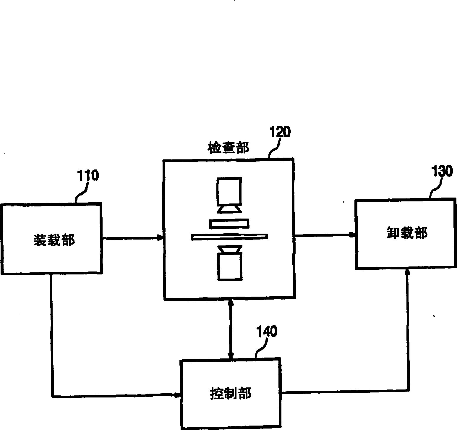
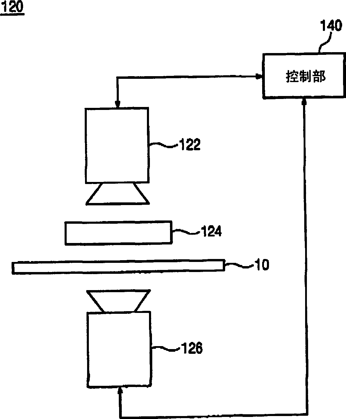
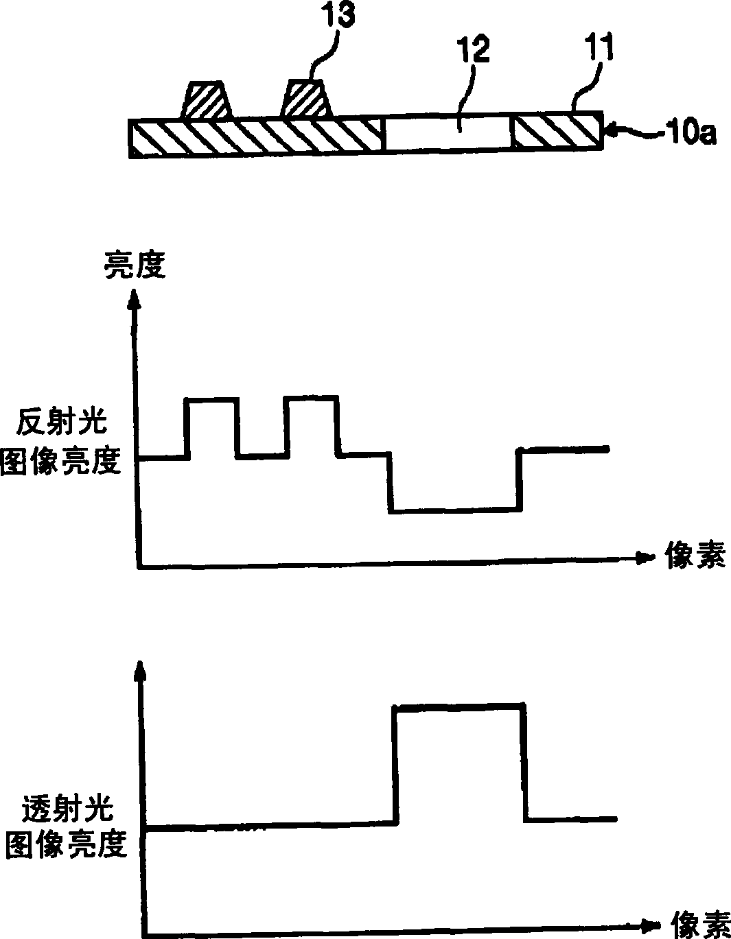
[0024] The inspection apparatus and method of the present invention are very suitable for simultaneously inspecting the appearance (foreign matter, discoloration, contamination, etc.) of a transmissive substrate and the burr of a through hole formed on the substrate.

[0025] figure 1 is a ...


PUM


Abstract

The invention provides an automatic optical inspection device of printed circuit substrate for inspecting the appearance of the inspected objects. The automatic optical inspection device of printed circuit substrate of the invention comprises: an illuminator for illuminating light to one side of the printed circuit substrate, a first shooting part for shooting the reflected image by using the reflected light reflected from one side of the printed circuit substrate, a second shooting part for shooting the transmission image using the transmission light transmitted from the side of the printed circuit substrate to the other side and a controlling part for receiving the reflected image and transmission image from the first and second shooting parts to judge whether there is foreign matter.

Description

technical field [0001] The present invention relates to an automatic optical inspection method, and more particularly, to an automatic optical inspection device and method for printed circuit boards for inspecting the appearance of inspection objects. Background technique [0002] Currently, among circuit boards (PCBs) for IC packaging, products such as Board On Chip (BOC) are generally used as memories. As a characteristic of this substrate, holes are usually drilled in the portion where the semiconductor chip is mounted. However, in the recent drilling process, there are often cut-off parts in the edge cross-section of the substrate, or fibrous foreign matter remains on the edge. Such foreign matter induces a fatal weakness, that is, the mountability is reduced when the semiconductor chip is post-mounted, and the inherent function (conductivity) is reduced after the semiconductor chip surface and the substrate pattern surface are mounted. [0003] Faced with such a situat...

Claims


Application Information

Patent Timeline
Patent Type & Authority Applications(China)
IPC IPC(8): G01N21/956G01B11/00
CPCG01B11/30G01N21/88G01N21/95684G06T2207/30141G06T7/70H05K3/0002
Inventor 崔铉镐金敏秀
Owner AJUHITEK
Why Eureka
Try Eureka