Semiconductor chip pickup apparatus and pickup method

A pick-up device and semiconductor technology, applied in semiconductor/solid-state device manufacturing, electrical components, circuits, etc., can solve the problems of semiconductor chip damage, maintaining sheet peeling residue, damage to semiconductor chips, etc., to achieve the effect of easy picking up

Inactive Publication Date: 2009-03-11
SHINKAWA CO LTD
View PDF1 Cites 15 Cited by
  • Summary
  • Abstract
  • Description
  • Claims
  • Application Information

AI Technical Summary

Problems solved by technology

[0004] However, there is the following problem in this method of protruding the ejector pin: if the thickness of the semiconductor chip becomes thinner, the problem of cracking the semiconductor chip due to the top will occur, and it is very difficult to pick up the thin semiconductor chip in recent years.
Especially in recent years, semiconductor chips are thin and have low strength, so cracks or deformation may occur due to such force
In this way, the method described in Patent Document 1 has the following problems: if a large suction hole is used, a large force is applied to the semiconductor chip during suction, and if a small suction hole is used, a large force is applied to the semiconductor chip when the base moves Larger force, therefore, the force applied to the semiconductor chip cannot be reduced when the holding sheet is peeled off, which can cause damage to the semiconductor chip
Therefore, if the suction hole is blocked by the peeled holding sheet due to the movement of the protrusion, the amount of air suction will gradually decrease, the degree of vacuum between the protrusion and the holding sheet will decrease, and the peeling force will gradually decrease.
In addition, on the side of the end face of the semiconductor chip toward the movement direction of the protruding part, the peeling residue of the holding sheet occurs, and the semiconductor chip cannot be picked up smoothly.
In this case, although the protruding height of the protruding portion can be increased, the peeling force of the holding sheet can be increased by utilizing the pulling force acting on the holding sheet, but, if there is a semiconductor chip adjacent to the moving direction of the protruding portion, sometimes The protruding portion collides with the semiconductor chip and damages the semiconductor chip, so the moving direction of the protruding portion is restricted

Method used


Image

  • Semiconductor chip pickup apparatus and pickup method
  • Semiconductor chip pickup apparatus and pickup method
  • Semiconductor chip pickup apparatus and pickup method

Examples


Embodiment Construction

[0082] Hereinafter, suitable embodiments of the present invention will be described with reference to the accompanying drawings. In the following embodiments, although various limitations are made to constituent elements, types, combinations, shapes, relative arrangements, etc., these are merely examples, and the present invention It is not limited to this.

[0083] Before describing the semiconductor chip pick-up device of the present invention, the wafer and the wafer holder will be described first.

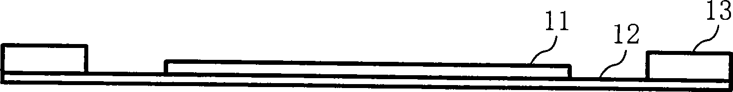
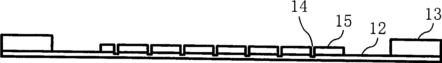
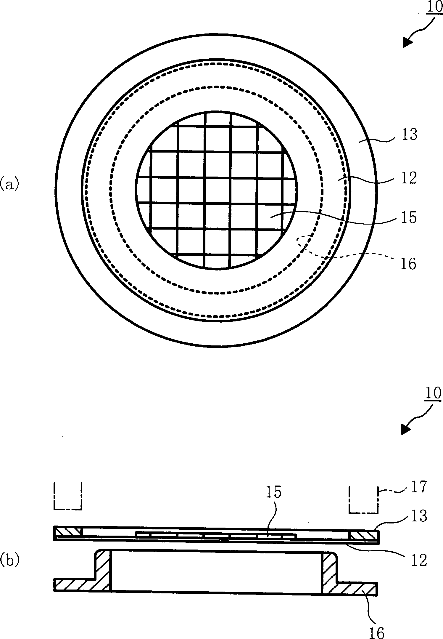
[0084] Such as figure 1 As shown, an adhesive holding sheet 12 is pasted on the back of the wafer 11 , and the holding sheet 12 is attached to a metal ring 13 . In this way, the wafer 11 is conveyed while being attached to the metal ring 13 via the holding sheet 12 . Then, if figure 2 As shown, in the cutting step, the wafer 11 is cut from the front side by a cutting blade or the like to form individual semiconductor chips 15 . Cut-in gaps 14 formed during dicing are form...


PUM


Abstract

The invention relates to a semiconductor die pick-up device and a pick-up method, providing a wiper (33) that has a tip end (33b) moving in and out of an adherence surface (22) and a shutter (23) that is moved with the wiper while blocking an opening (41) located on moving direction of the wiper. When picking up a semiconductor die (15), the tip end of the wiper is aligned with one end (15a) of the semiconductor die; the wiper (33) is moved along the adherence surface (22) while the tip end of the wiper is protruded from the adherence surface with the semiconductor die being suction-held by a collet (18); a suction opening (42) is sequentially opened between an end surface (41a) of the opening (41) and a sheet surface (33a); a dicing sheet (12) is sequentially sucked from one end (15a) of the semiconductor die (15) at the suction opening and is sequentially peeled from the semiconductor die (15). In the pick-up device of the semiconductor die, effects of inhibiting the power exerted onto a semiconductor die when peeling a dicing sheet and of easily picking up a semiconductor die are provided.

Description

technical field [0001] The present invention relates to a structure and a pick-up method of a semiconductor chip (die) pick-up device. Background technique [0002] Semiconductor chips are manufactured by cutting a 6-inch or 8-inch wafer into a predetermined size. When dicing, in order to prevent the diced semiconductor chips from being messed up, an adhesive holding sheet is attached to the back surface, and the wafer is cut from the front side with a cutting blade or the like. At this time, the holding sheet attached to the back surface is not cut, although it is slightly cut, and each semiconductor chip is held. Then, the cut semiconductor chips are picked up from the holding sheet one by one, and sent to the next process such as die bonding. [0003] In the past, as a method of picking up a semiconductor chip from an adhesive holding sheet, the method of protruding pins is mostly used (for example, referring to Patent Document 1 Figure 15 ). This method is to use a c...

Claims


Application Information

Patent Timeline
Patent Type & Authority Applications(China)
IPC IPC(8): H01L21/00
CPCY10T156/1983H01L21/67132H01L21/52H01L21/67144H01L21/67706H01L21/67712H01L21/67721H01L21/6838H05K13/0408
Inventor 藤野昇梅原沖人胜吕明男佐佐木真一
Owner SHINKAWA CO LTD
Why Eureka
Try Eureka