Organic electroluminescence device and method for manufacturing the same

A technology of electroluminescent devices and organic light-emitting layers, which is applied in semiconductor/solid-state device manufacturing, electric solid-state devices, electrical components, etc., can solve problems such as damage to thin-film transistors, and achieve the effect of improving interface characteristics and increasing electrical contact

Active Publication Date: 2009-03-18
LG DISPLAY CO LTD
View PDF2 Cites 5 Cited by
  • Summary
  • Abstract
  • Description
  • Claims
  • Application Information

AI Technical Summary

Problems solved by technology

[0012] In a conventional active matrix type organic electroluminescent device, the thin film transistor is exposed to X-rays or the like during the deposition process of the anode, light emitting layer and cathode, thereby causing damage to the thin film transistor

Method used


Image

  • Organic electroluminescence device and method for manufacturing the same
  • Organic electroluminescence device and method for manufacturing the same
  • Organic electroluminescence device and method for manufacturing the same

Examples


Embodiment Construction

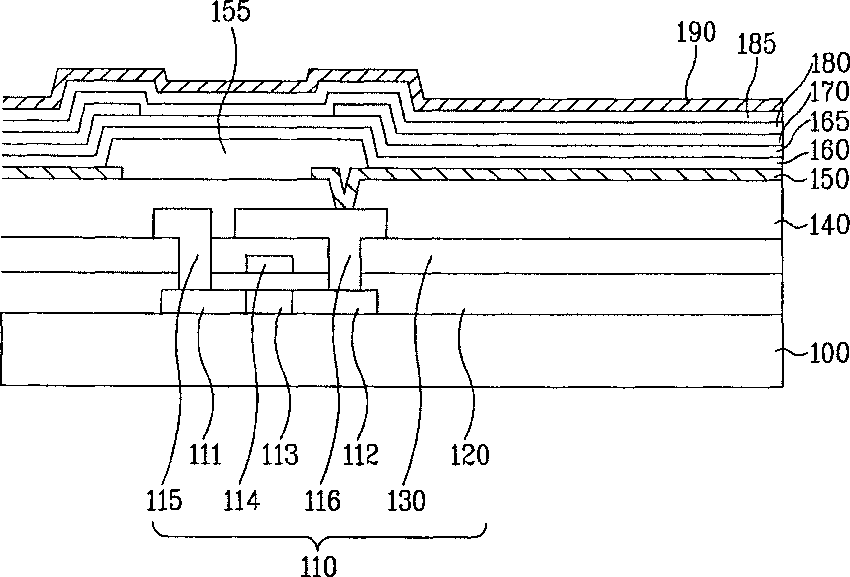
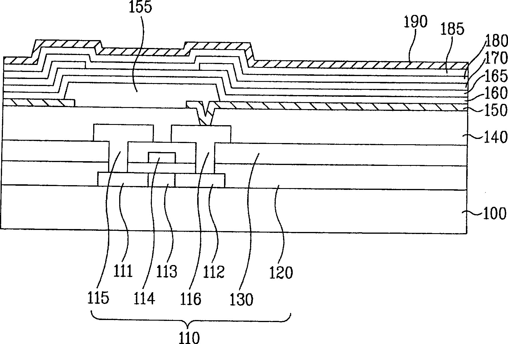
[0027] Reference will now be made in detail to the preferred embodiments of the invention, examples of which are illustrated in the accompanying drawings. Wherever possible, the same reference numbers will be used throughout the drawings to refer to the same or like parts.

[0028] Hereinafter, an organic electroluminescence device and a manufacturing method thereof according to the present invention will be described in detail with reference to the accompanying drawings.

[0029] The dimensions of thickness are exaggerated in the drawings to clearly show several layers and regions. The thickness ratios of the respective layers shown in the drawings are not equal to the actual thickness ratios. Meanwhile, when a part such as a layer, a film, a region, and a plate is formed or provided "on" another part, it should be understood that the part may be directly formed on the other part by direct contact, or may be provided with another part in between. part.

[0030] figure 1 ...


PUM


Abstract

An organic electroluminescence device and a method for manufacturing the same are disclosed. The organic electroluminescence device includes a transparent substrate, a semiconductor layer including a source region, a channel region and a drain region, a gate insulating film having first contact holes on the source and drain regions and formed on the substrate including the semiconductor layer, a gate electrode formed on the gate insulating film above the channel region, an interlayer insulating film having second contact holes on the source and drain regions and formed on an entire surface of the gate insulating film including the gate electrode, and a source electrode and a drain electrode formed on the interlayer insulating film to be electrically connected to the source and drain regions through the first and second contact holes, wherein at least one of the source electrode and the drain electrode is formed to cover the semiconductor layer.

Description

[0001] Cross References to Related Applications [0002] This application claims the benefit of Korean Patent Application No. 10-2007-0093077 filed on September 13, 2007, and Korean Patent Application No. 10-2008-0080687 filed on August 19, 2008, which are hereby incorporated in their entirety For reference, like listing them all here. technical field [0003] The present invention relates to an organic electroluminescent device and a manufacturing method thereof, in particular to an electrode structure of a thin film transistor used as a driving switch in an organic electroluminescent device and a method for manufacturing the organic electroluminescent device. Background technique [0004] In the multimedia era, display devices need to be thinner and larger and capable of displaying colors close to natural colors. Conventional cathode ray tubes (CRTs) are limited in providing large screens of 40 inches or more. Organic electroluminescence devices, liquid crystal display ...

Claims


Application Information

Patent Timeline
Patent Type & Authority Applications(China)
IPC IPC(8): H01L27/32H01L29/786H01L29/43H01L29/417H01L21/84H01L21/336H01L21/28
CPCH01L2924/12044H10K59/123H10K59/124H10K50/81H10K50/82H10K50/11H10K71/00
Inventor 郑然植许峻瑛
Owner LG DISPLAY CO LTD
Why Eureka
Try Eureka