Anode for secondary battery, its manufacturing method and secondary battery
A secondary battery and manufacturing method technology, applied in the direction of electrode manufacturing, secondary batteries, battery electrodes, etc., can solve the problems of not being able to obtain sufficient charge-discharge cycle characteristics, difficulties, etc., and achieve the effect of excellent charge-discharge cycle performance
- Summary
- Abstract
- Description
- Claims
- Application Information
AI Technical Summary
Problems solved by technology
Method used
Image
Examples
Embodiment 1~3
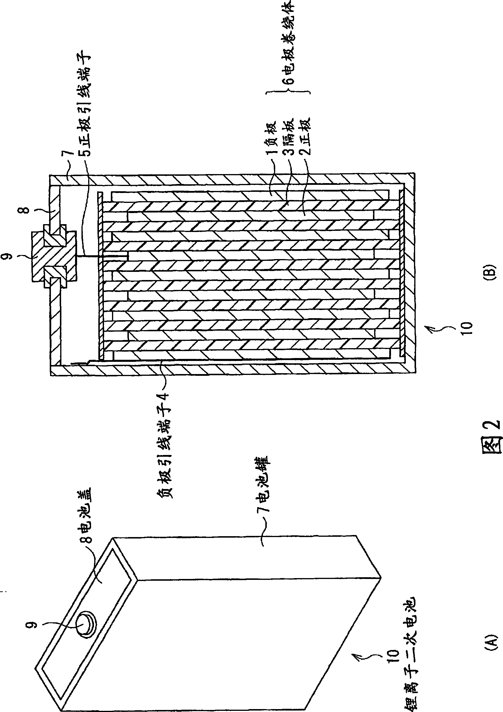
[0153] In this embodiment, a negative electrode active material layer is formed on the negative electrode current collector by vacuum evaporation, and it is used as the negative electrode 1 to make the square lithium ion secondary battery 10 shown in FIG. 2 in the embodiment. , and measured its charge-discharge cycle characteristics. Below, it demonstrates concretely.
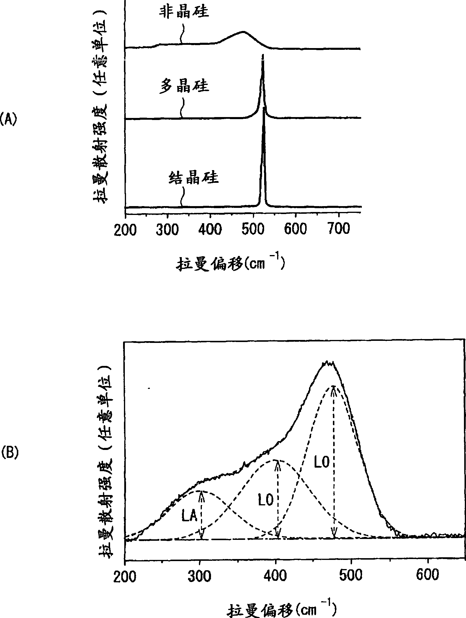
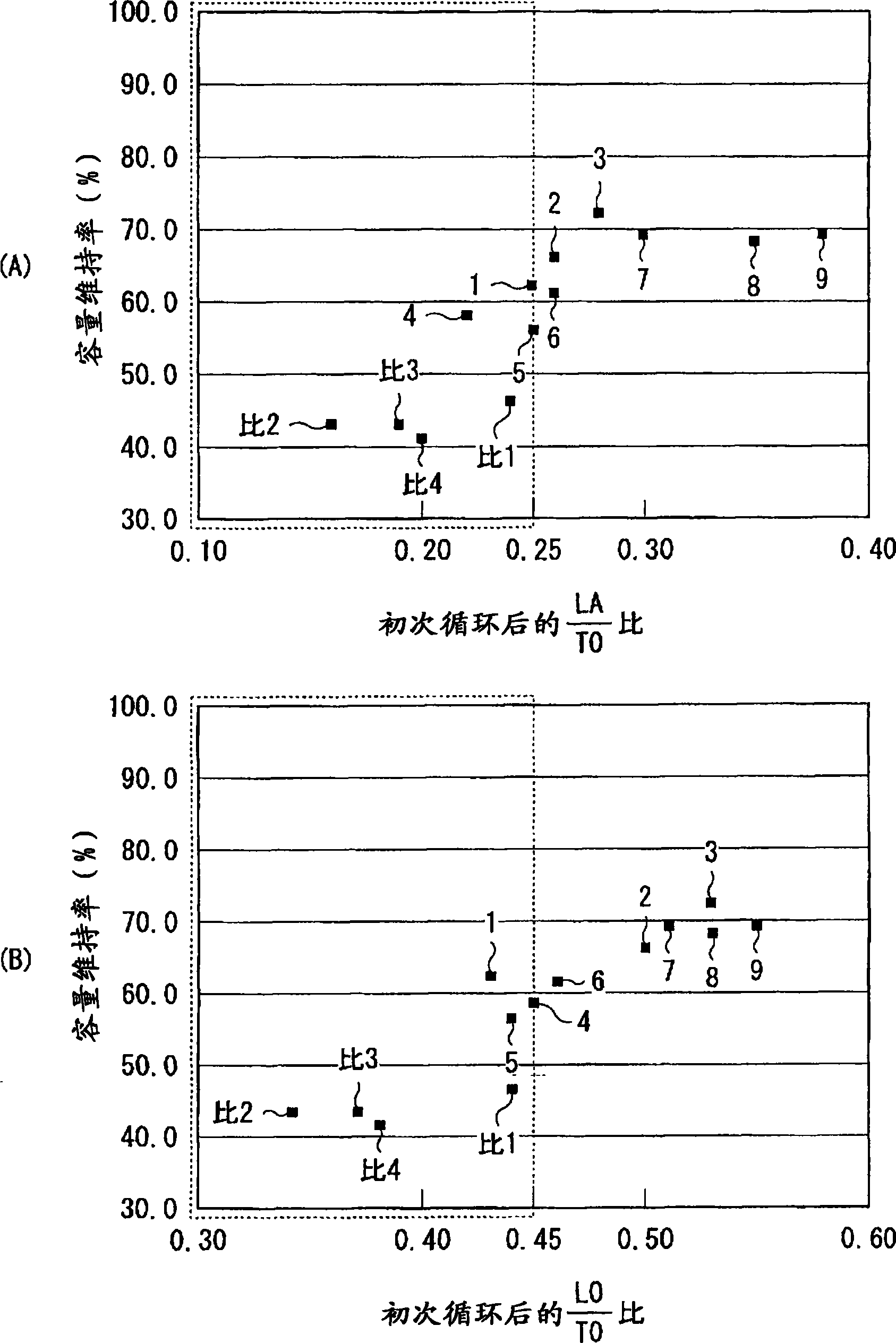
[0154] First, negative electrode 1 having amorphous silicon having different degrees of local order as a negative electrode active material layer was fabricated as follows.
[0155] When forming the negative electrode 1 , a vacuum vapor deposition device shown in FIG. 5 was used as an electrode forming device. A strip-shaped electrolytic copper foil having a thickness of 24 μm, a surface roughness Rz value of 2.5 μm, and roughening on both sides was used as the negative electrode current collector; a silicon single crystal was used as the vapor deposition material. The film forming speed was set at 50-100 nm / ...
Embodiment 4~9
[0186]In this example, the lithium ion secondary battery 10 was fabricated in the same manner as in Examples 1 to 3 except that the negative electrode active material layer was formed by the sputtering method.
[0187] When forming the negative electrode 1 , a facing target type DC sputtering device (not shown) was used as an electrode forming device. A strip-shaped electrolytic copper foil with a thickness of 24 μm, a surface roughness Rz value of 2.5 μm, and roughened on both sides was used as the negative electrode current collector, and a silicon single crystal was used as the vapor deposition material. The film formation rate was 0.5 nm / s, and a negative electrode active material layer with a thickness of 5 to 6 μm was formed. At this time, the DC power was 1kW, argon gas was used as the discharge gas, and negative electrode active material layers with various levels of local order were formed by adjusting film formation conditions such as negative electrode current colle...
Embodiment 10~16
[0201] In this example, as in examples 1 to 3, a negative electrode active material layer was formed by a vacuum evaporation method to fabricate a lithium ion secondary battery 10 . The difference from Examples 1 to 3 is that oxygen is directly introduced into the flow of the vapor deposition material of silicon from the vapor deposition source to the negative electrode current collector, and negative electrode active material layers having different oxygen contents are formed. The film forming speed is fixed at 50nm / s. The temperature of the negative electrode current collector and the flow rate of oxygen were as follows.
PUM
| Property | Measurement | Unit |
|---|---|---|
| thickness | aaaaa | aaaaa |
| thickness | aaaaa | aaaaa |
| thickness | aaaaa | aaaaa |
Abstract
Description
Claims
Application Information


