Tool plate and test method using the same

A tool and test point technology, applied in the field of testing, can solve problems affecting the miniaturization of electronic products, and achieve the effects of reducing design difficulty and production cost, increasing service life, and reducing production and testing costs

Inactive Publication Date: 2009-04-01
HUAWEI DEVICE (SHENZHEN) CO LTD
View PDF0 Cites 1 Cited by
  • Summary
  • Abstract
  • Description
  • Claims
  • Application Information

AI Technical Summary

Problems solved by technology

[0006] In view of this, the embodiment of the present invention provides a tool board and a testing method using it to solve the problem that a single board affects the miniaturization of electronic products

Method used


Image

  • Tool plate and test method using the same
  • Tool plate and test method using the same
  • Tool plate and test method using the same

Examples


Embodiment Construction

[0022] In order to make the above features and advantages of the embodiments of the present invention more obvious and understandable, the embodiments of the present invention will be described in detail below in conjunction with specific implementations.

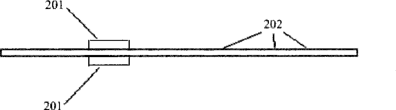
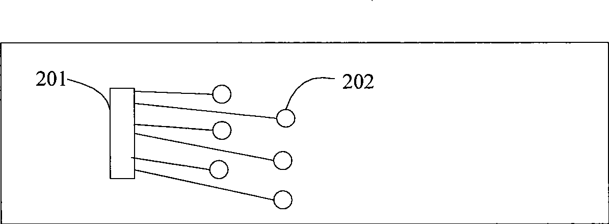
[0023] Please refer to Fig. 2 (a), which is a side view of the tool board structure of the embodiment of the present invention, please refer to Fig. 2 (b), which is a top view of the tool board structure of the embodiment of the present invention, the tool board of the embodiment of the present invention may include:

[0024] At least one connector 201: matching with the connector on the single board, leading the test signal of the single board to at least one test point without affecting the function of the single board;

[0025] At least one test point 202: arranged on the tool board, for providing the test signal to the test pin.

[0026] The tool board shown in Fig. 2 will be described in detail below.

[0027] The too...


PUM


Abstract

The invention discloses a tool board and a method of conducting tests via the tool board. The tool board includes: at least one linker, which is matched with a linker on a veneer and used for leading a test signal on the veneer out to at least one testing point. The one testing point is arranged on the tool board and used for providing a testing needle with the test signal. The method of conducting tests via the tool board comprises the following steps: the veneer is installed on the tool board; the linker on the tool board leads the test signal on the veneer out to the testing points on the tool board; the veneer is tested through the testing points. In virtue of the invention, the bulk of an electronic product can be effectively reduced.

Description

technical field [0001] The invention relates to the technical field of testing, in particular to a tool board and a testing method using it. Background technique [0002] During the production process of a single board of an electronic product, several test points are usually arranged to provide testers with test signals or electrical signals. In the case of a large board, the test points arranged on the board can be as large as possible, so that the tester can test and avoid misoperation. [0003] Due to the shrinkage of electronic products, single boards are also getting smaller and smaller, and single boards connected by connectors appear. Please refer to figure 1 as shown, figure 1 It is a schematic diagram of a board composed of two boards connected by a connector, and the upper and lower boards are connected by a B2B connector. Since the upper and lower veneers are very small, in order to ensure that the test pins of the fixture can touch the test points, the test ...

Claims


Application Information

Patent Timeline
Patent Type & Authority Applications(China)
IPC IPC(8): G01R1/02G01R31/00
Inventor 翟巍
Owner HUAWEI DEVICE (SHENZHEN) CO LTD
Why Eureka
Try Eureka