

Solid-state imaging device, method of driving solid-state imaging device, method of manufacturing solid-state imaging device, and electronic apparatus
a technology of solid-state imaging and manufacturing methods, applied in the direction of transistors, television systems, radio control devices, etc., can solve the problem of low ease of such a configuration, and achieve the effect of eliminating a potential barrier h2 and eliminating a potential barrier
Active Publication Date: 2016-11-17
SONY SEMICON SOLUTIONS CORP
View PDF6 Cites 33 Cited by
- Summary
- Abstract
- Description
- Claims
- Application Information
AI Technical Summary
Benefits of technology
The invention provides a solid-state imaging device that can save space by stacking multiple photodiodes, a method of driving and manufacturing the device, as well as an electronic apparatus. The plurality of photodiodes can also act as a transfer path for signal charge, reducing the space needed for transistors and making the design easier. Overall, the invention allows for a more efficient use of space when creating a solid-state imaging device.
Problems solved by technology
Moreover, it is not easy to form the vertical transistor so as to extend a gate electrode from a circuit formation surface to a photodiode disposed in a deepest region; therefore, feasibility of such a configuration is low.
Method used
View moreImage
Smart ImageViewing Examples

Examples
first embodiment (
1. First Embodiment (An example of a solid-state imaging device in which a vertical transistor and a wiring layer are embedded in a semiconductor layer)
modification example 1 (
2. Modification Example 1 (An example of a manufacturing method in a case in which photodiodes are stacked by substrate bonding)
second embodiment (
3. Second Embodiment (An example of a solid-state imaging device that performs electric charge transfer with use of a separation layer (a diffusion layer) between photodiodes without using a vertical transistor)
Login to View More PUM
 Abstract
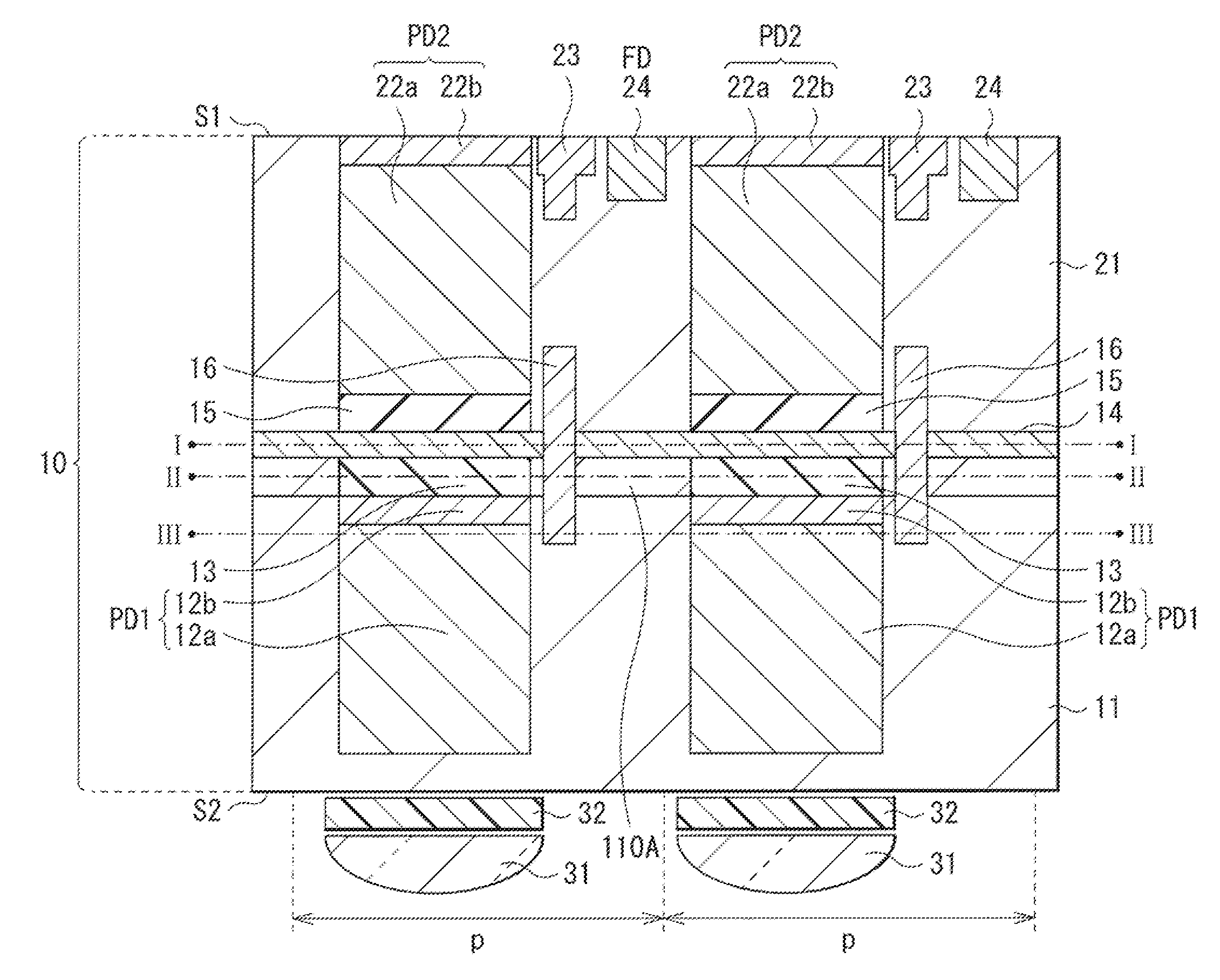
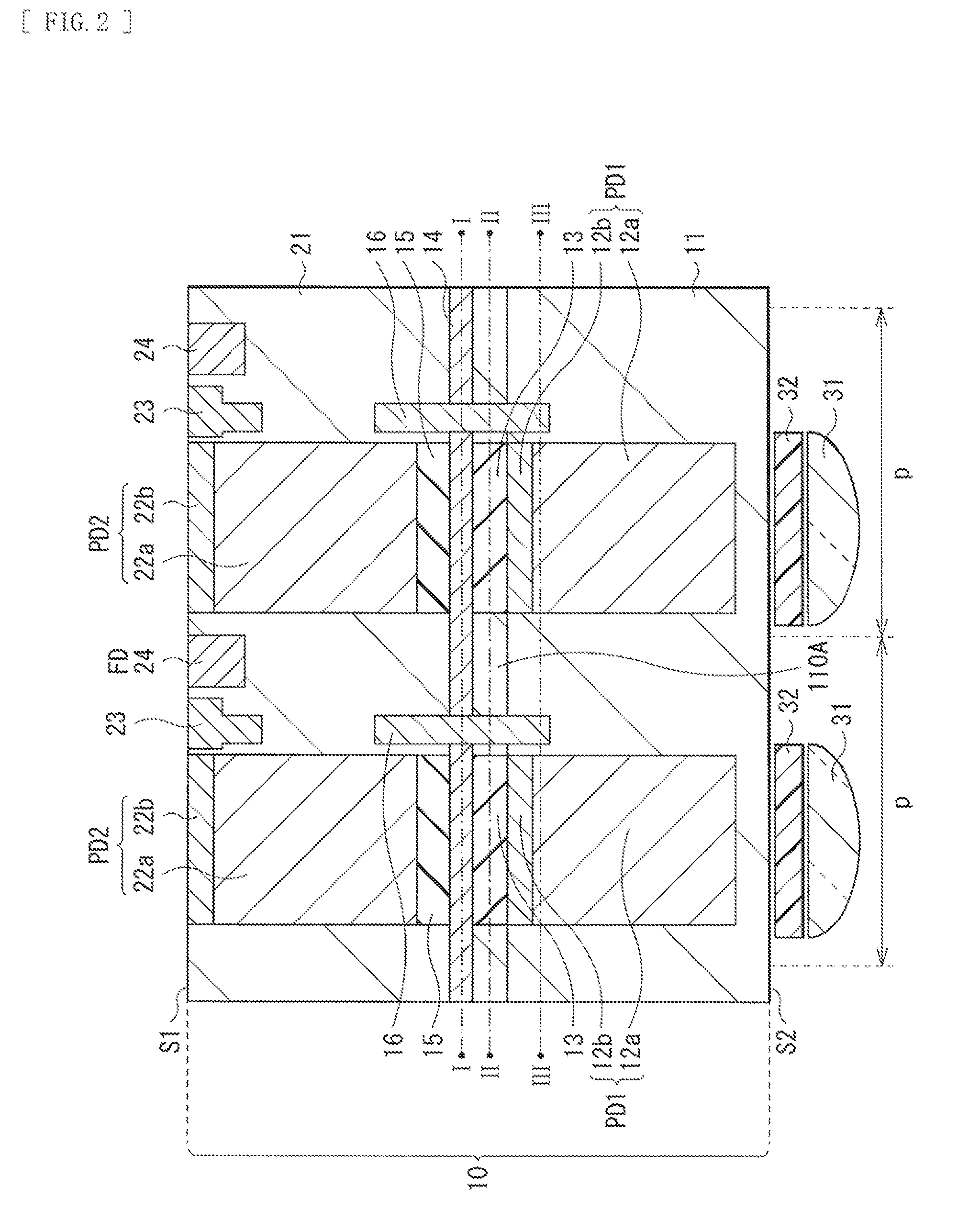
A solid-state imaging device includes: a semiconductor layer having a first surface and a second surface that oppose each other; and a plurality of photodiodes stacked in the semiconductor layer. One or more photodiodes of the plurality of photodiodes also serve as a transfer path of a signal charge accumulated in other photodiodes.
Description
TECHNICAL FIELD[0001]The disclosure relates to a solid-state imaging device used for, for example, a CCD (charge coupled device) or a CMOS (complementary metal oxide semiconductor) image sensor, a method of driving a solid-state imaging device, a method of manufacturing a solid-state imaging device, and an electronic apparatus.BACKGROUND ART[0002]In solid-state imaging devices used for CCDs, CMOS image sensors, and other image sensors, so-called vertical transistors have been practically used as switching elements for reading of a signal charge from a photodiode (PD).[0003]The vertical transistors each include an electrode (a gate electrode) embedded in a depth (thickness) direction in a semiconductor substrate made of silicon (Si) or any other semiconductor. Using the vertical transistor makes it possible to read out a signal charge from a photodiode that is disposed in a deep region in the semiconductor substrate. Moreover, using the vertical transistor also makes it possible to r...
Claims
Login to View More Application Information
Patent Timeline
 IPC IPC(8): H04N5/378H01L27/146
CPCH04N5/378H01L27/14647H01L27/14636H01L27/14612H01L27/14689H01L27/14623H01L27/1464H01L27/14634H01L27/1469H01L27/14621H01L27/14627H01L27/14638H01L27/14645H04N25/75
InventorITO, KYOSUKE
OwnerSONY SEMICON SOLUTIONS CORP