Pure metal oxide semiconductor (MOS) structure voltage reference source with high power supply rejection ratio

A high power supply rejection ratio, MOS structure technology, applied in the direction of adjusting electrical variables, control/regulation systems, instruments, etc., can solve the problems of increasing quiescent current, high process cost, reducing start-up circuits, etc., to improve voltage suppression performance, reduce The difficulty of circuit design and the effect of high power supply rejection ratio

Active Publication Date: 2014-01-22
SOUTHEAST UNIV
View PDF5 Cites 33 Cited by
  • Summary
  • Abstract
  • Description
  • Claims
  • Application Information

AI Technical Summary

Problems solved by technology

The second type needs to implement enhancement mode and depletion mode MOS devices on the same silicon chip. The chip manufacturing process requires an additional mask, which also has special requirements for the process, the process cost is high, and there is a large deviation with the process angle; the third type Using the gate-source voltage difference of MOS devices to realize the reference, there is no special requirement for the process, but a stable peripheral bias circuit is required and the process angle deviation is still large
Although the second type requires corresponding process support, the use of depletion-type MOS devices to generate voltage references will reduce the corresponding start-up circuits, while the circuit is simple, and can achieve a lower power supply voltage power supply reference
The third type has no special requirements on the process, but its temperature coefficient is also affected by nonlinear factors such as carrier mobility.
But complex operational amplifiers increase the difficulty of design, while adding a large amount of quiescent current

Method used


Image

  • Pure metal oxide semiconductor (MOS) structure voltage reference source with high power supply rejection ratio
  • Pure metal oxide semiconductor (MOS) structure voltage reference source with high power supply rejection ratio
  • Pure metal oxide semiconductor (MOS) structure voltage reference source with high power supply rejection ratio

Examples


Embodiment Construction

[0021] The principles and features of the present invention will be described below in conjunction with the accompanying drawings, and the examples given are only used to explain the present invention, and are not intended to limit the scope of the present invention.

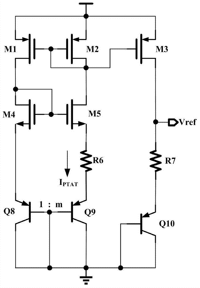
[0022] Such as figure 1, is a traditional bandgap reference circuit using transistors and resistors as the core. It is a transistor base-emitter voltage VBE with a negative temperature coefficient and a thermal voltage VT with a positive temperature coefficient. The voltage is weighted and added to obtain an output voltage with zero temperature coefficient, but in the CMOS process, the triode has problems such as too large area and high power consumption, and the model of the parasitic triode is not accurate enough.

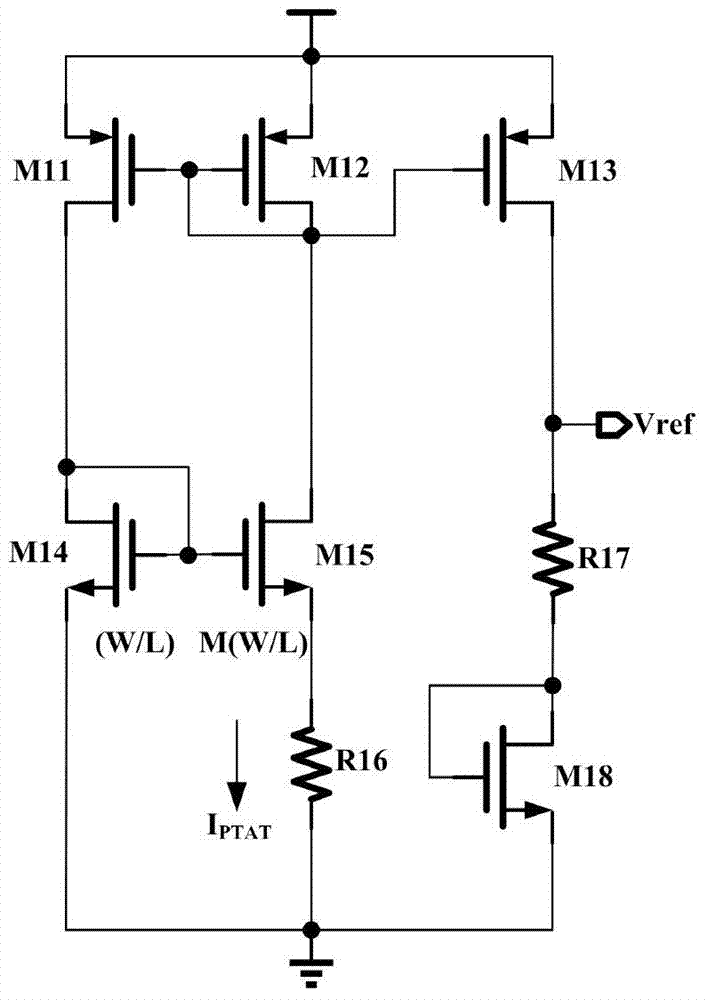
[0023] Such as figure 2 , is a voltage reference circuit using MOS tubes and resistors as the core, wherein MOS tubes M14 and M15 work in the sub-threshold region. This circuit uses the negative...


PUM


Abstract

A pure metal oxide semiconductor (MOS) structure voltage reference source with high power supply rejection ratio (PSRR) comprises a starting circuit, an IPTAT generation circuit, a VPTAT generation circuit, a VGS generation circuit and a PSRR reinforcing feedback circuit. The starting circuit is connected with the IPTAT generation circuit, the output of the IPTAT generation circuit is connected with the VPTAT generation circuit and the VGS generation circuit, the output of the VPTAT generation circuit and the output of the VGS generation circuit are overlapped to form Vref reference voltage output, and the output reference voltage is fed back to the IPTAT generation circuit through the PSRR reinforcing feedback circuit to generate a circuit to form a closed feedback loop.

Description

technical field [0001] The invention belongs to the technical field of analog integrated voltage reference source circuits, and in particular relates to a pure MOS structure voltage reference source with high power supply rejection ratio. Background technique [0002] In the design of analog circuits, digital-analog hybrid integrated circuits or system chips, it is often necessary to use a reference voltage source, which converts the power supply voltage into a reference voltage that is approximately independent of the power supply voltage and temperature, and is used to provide stable bias for other parts of the circuit. setting and reference voltage. Therefore, the low temperature drift coefficient and high voltage rejection ratio are the key performance indicators of the voltage reference source. In the digital-analog hybrid integrated circuit, the noise of the digital part is easily coupled into the power supply, so the requirements for the circuit power supply suppress...

Claims


Application Information

Patent Timeline
Patent Type & Authority Applications(China)
IPC IPC(8): G05F1/567
Inventor 孙伟锋杨棒张允武祝靖刘斯扬陆生礼时龙兴
Owner SOUTHEAST UNIV
Why Eureka
Try Eureka