Chip electro-static discharge test device

An electrostatic discharge test and chip technology, applied in the direction of measuring devices, measuring electricity, measuring electrical variables, etc., can solve the problems of ESD equipment without test board, long test board cycle, high cost, etc., to achieve short cycle, low production cost, cost reduction effect

Inactive Publication Date: 2009-04-01
VIMICRO CORP
View PDF0 Cites 15 Cited by
  • Summary
  • Abstract
  • Description
  • Claims
  • Application Information

AI Technical Summary

Problems solved by technology

However, for ICs in special packages, due to their special pin distribution and other issues, ESD equipment does not have a matching test board, which requires a custom-made

Method used


Image

  • Chip electro-static discharge test device
  • Chip electro-static discharge test device
  • Chip electro-static discharge test device

Examples


Embodiment 1

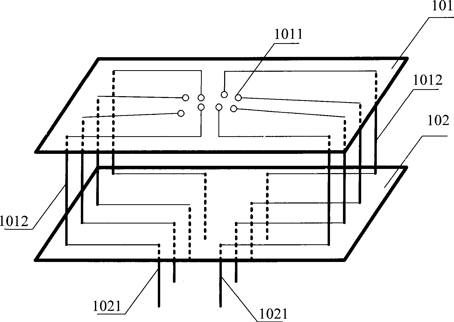
[0027] refer to figure 1 , which shows Embodiment 1 of the chip ESD testing device of the present invention, which may specifically include:

[0028] Circuit board 101 and circuit board 102;

[0029] The upper surface of the circuit board 101 is provided with welding pads 1011 corresponding to the positions of the respective pins of the chip to be tested; the soldering pads 1011 are used for electrical connection with each pin of the chip to be tested during testing.

[0030] Both sides of the circuit board 101 are provided with pin headers 1012 that are electrically connected one-to-one with the solder pads 1011; wherein, the electrical connection between the solder pads 1011 and the pin headers 1012 is realized through the wiring on the circuit board 101, and the circuit board 101 may be a PCB (Print circuit board, printed circuit board) board.

[0031] The other end of the pin header 1012 is electrically connected to the circuit board 102, and the lower surface of the cir...

Embodiment 3

[0038] refer to Figure 4 , showing another chip ESD testing device embodiment 3, specifically may include:

[0039] A circuit board 401, the upper surface of the circuit board 401 is provided with a welding pad 4011 corresponding to each pin position of the chip to be tested; the welding pad 4011 is used for electrical connection with each pin of the chip to be tested during testing;

[0040] The lower surface of the circuit board 401 is provided with a pin header 4012 corresponding to a chip-on-board (COB, Chip on Board) test board; the welding pad 4011 is electrically connected to the pin header 4012 one-to-one. The circuit board 401 may be a PCB board. Among them, the COB test board can be used for ESD testing on chips with 256 pins at most.

[0041]When testing, the chip to be tested is directly welded on the circuit board 401 , so that each pin of the chip is electrically connected to the pad 4011 .

[0042] The device can also have the following purposes: when ESD fa...


PUM

PropertyMeasurementUnit
Resistanceaaaaaaaaaa

Abstract

The invention provides a device for testing the static discharge of a chip. The device comprises a first circuit board and a second circuit board; the upper surface of the first circuit board is provided with pads corresponding to the positions of all pins of the chip to be tested, and the pads are used for electrically connecting each pin of the chip to be tested when welding; the two sides of the first circuit board are provided with a faller A which is electrically connected with the pads in an one-to-one way; the other end of the faller A is electrically connected with a second circuit board, the lower surface of the second circuit board is provided with a faller B corresponding to a testing board of the static discharge testing equipment, the faller A and the faller B are electrically connected in a one-to-one way. By adopting the invention, the testing device suitable for special encapsulated chips can be manufactured according to the testing board in the testing equipment, thus realizing that all measured pins of the chip to be tested are electrically connected with the inside of the testing equipment. The testing device has simple structure and design, low manufacturing cost and short manufacturing period and reduces the cost for carrying out the static discharge test on the special encapsulated chips.

Description

technical field [0001] The invention relates to the technical field of chip testing, in particular to a chip electrostatic discharge testing device. Background technique [0002] Electrostatic Discharge (ESD, Electrostatic Discharge) is one of the most costly damage causes in the electronics industry. It will affect the production yield, manufacturing cost, product quality and reliability, and the company's profitability. Therefore, it is necessary to conduct ESD tests on IC products to evaluate their ESD protection performance. [0003] At present, domestic ESD tests are generally carried out with standard ESD test equipment, and these test equipment need to place the IC on a test board that matches the package form of the IC when performing ESD testing, so that all the pins to be tested can pass the test The board is electrically connected to the inside of the device. [0004] Usually ESD test equipment will be equipped with several test boards suitable for more commonly...

Claims


Application Information

Patent Timeline
IPC IPC(8): G01R31/00
Inventor 宋鑫欣
Owner VIMICRO CORP
Why Eureka
Try Eureka