Array substrate of LCD

A liquid crystal display, array substrate technology, applied in the direction of instruments, nonlinear optics, optics, etc., can solve the problems of reducing the performance of left and right viewing angles, light leakage, and reducing the aperture ratio, and achieve the effect of avoiding light leakage

Inactive Publication Date: 2009-04-01
BEIJING BOE OPTOELECTRONCIS TECH CO LTD
View PDF0 Cites 4 Cited by
  • Summary
  • Abstract
  • Description
  • Claims
  • Application Information

AI Technical Summary

Problems solved by technology

When the liquid crystal display panel is tapped, the alignment of the color filter substrate and the array substrate is distorted, that is, the black matrix 6 and the data line 3 are dislocated and moved, causing the light between the shielding strip 2 and the data line 3 to leak out, resulting in light leakage. , resulting in the appearance of water ripples (TouchMura), leading to the result of reducing the performance of the left and right viewing angles, such as figure 2 shown
[0003] In order to solve the above-mentioned problems, methods such as increasing the width of the black matrix and increasing the width of the shielding strips are usually adopted in the prior art, but the above-mentioned technical solutions not only cannot completely prevent the occurrence of light leakage caused by the offset of the black matrix when the liquid crystal display panel is tapped, And it will also have the negative impact of reducing the opening ratio

Method used


Image

  • Array substrate of LCD
  • Array substrate of LCD
  • Array substrate of LCD

Examples


Embodiment Construction

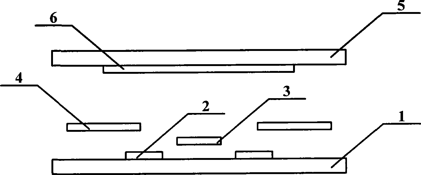
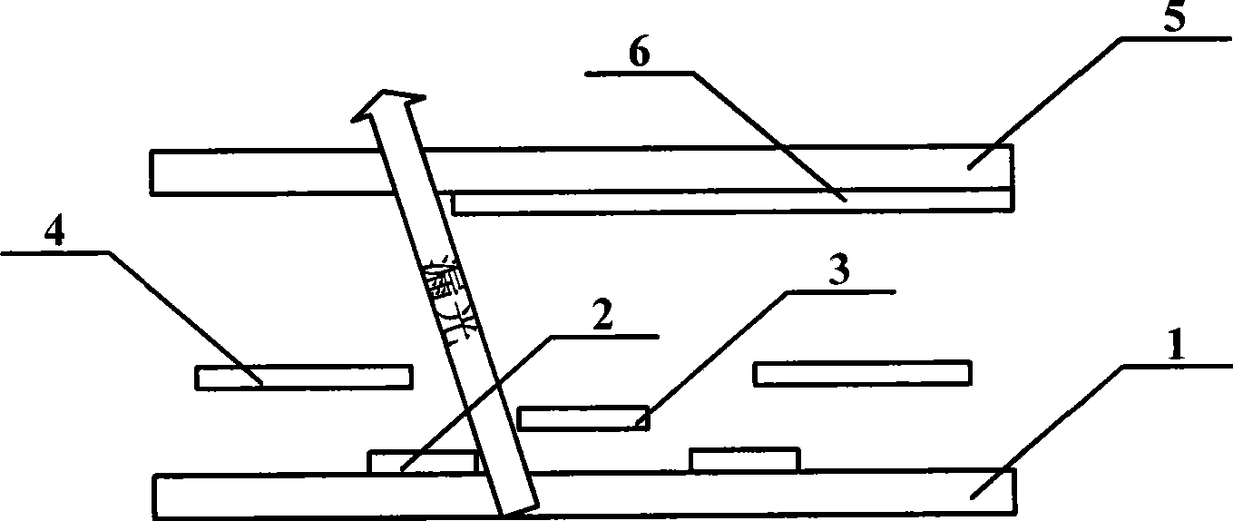
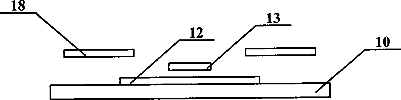
[0011] Such as image 3 As shown, it is a schematic cross-sectional structure diagram of the data line direction of the specific embodiment of the array substrate of the liquid crystal display of the present invention. This embodiment includes a substrate 10, on which gate lines (not shown) and data lines 13 intersecting each other to define a pixel area are provided, and a pixel electrode 18 is provided in the pixel area, wherein: the data lines Shielding strips 12 are arranged in parallel directly below, and the width of the shielding strips 12 is greater than that of the data lines 13 .

[0012] In the present invention, the shielding bar with a width greater than the width of the data line is arranged in parallel directly under the data line, so that no light leakage occurs around the data line, and the light leakage that may occur when the panel is tapped is effectively avoided.

[0013] In order to further avoid short-circuit and disconnection of the data line, in this ...


PUM


Abstract

The invention relates to an array substrate of an LCD. The array substrate comprises a substrate which is provided with a plurality of grid lines and data lines which cross each other to define pixel areas; each pixel area is provided with a pixel electrode, wherein, shielding strips are arranged in parallel just below the data lines, and the width of the shielding strips is greater than that of the data lines. The shielding strips are connected with the data lines through holes. By arranging shielding strips which are wider than the data lines in parallel just below the data lines, the array substrate effectively avoids the light leakage that possibly occurs while flapping a panel.

Description

technical field [0001] The invention relates to an array substrate, which belongs to the field of manufacturing liquid crystal display devices. Background technique [0002] The core component used in the manufacturing process of a liquid crystal display (Liquid Crystal Display, hereinafter referred to as LCD) is a liquid crystal display panel composed of an array substrate and a color filter substrate. Such as figure 1 As shown in FIG. 1 , is a schematic diagram of a cross-sectional structure of a liquid crystal display panel in the prior art in the direction of data lines. The array substrate includes a first substrate 1, on which shielding strips 2, gate lines (not shown in the figure), data lines 3 and pixel electrodes Indium Tin Oxide (Indium Tin Oxide, hereinafter referred to as ITO) 4 are arranged; The film substrate includes a second substrate 5 on which a black matrix (Black matrix, BM for short) 6 and a color resin (Color Resin) are arranged. When the liquid cry...

Claims


Application Information

Patent Timeline
Patent Type & Authority Applications(China)
IPC IPC(8): G02F1/1362
Inventor 田正牧
Owner BEIJING BOE OPTOELECTRONCIS TECH CO LTD
Why Eureka
Try Eureka