Thinning method for backing side of wafer
A backside thinning and wafer technology, applied in electrical components, semiconductor/solid-state device manufacturing, circuits, etc., can solve problems such as wafer edge bending and fracture, and achieve the effect of improving quality
- Summary
- Abstract
- Description
- Claims
- Application Information
AI Technical Summary
Problems solved by technology
Method used
Image

Examples
Embodiment approach
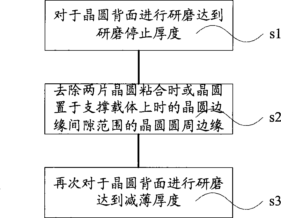
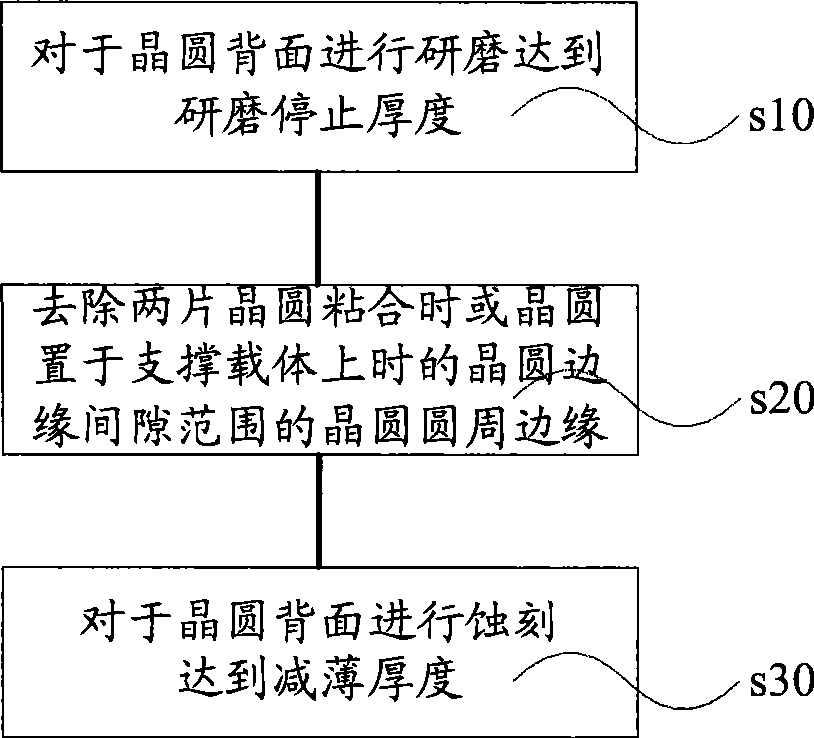
[0062] Refer to image 3 As shown, another embodiment of the wafer backside thinning method of the present invention includes the following steps:
[0063] Step s10, grinding the back of the wafer to reach the grinding stop thickness;
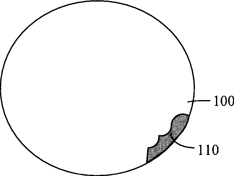
[0064] Step s20, removing the peripheral edge of the wafer in the wafer edge gap range when the two wafers are bonded or when the wafer is placed on the support carrier;
[0065] Step s30, etching the backside of the wafer to reduce the thickness.
[0066] Each step will be further explained below.
[0067] For step s10, the grinding stop thickness is 100 to 200um.
[0068] For step s20, an etching method is used to remove the peripheral edge of the wafer in the gap range of the wafer edge when the two wafers are bonded or when the wafer is placed on the support carrier. In addition, the above-mentioned etching method is a method of ion reactive etching.
[0069] The ion reactive etching method includes the following steps:
[0070] Form a photoresis...
PUM
 Abstract
Description
Claims
Application Information