

Chemical mechanical grinding method
A grinding method and chemical mechanical technology, which is applied in the direction of grinding devices, grinding machine tools, grinding/polishing equipment, etc., can solve the problem that the layer to be ground is not completely removed, and achieve the effect of improving uniformity and consistency and good grinding effect
- Summary
- Abstract
- Description
- Claims
- Application Information
AI Technical Summary
Problems solved by technology
Method used
Image

Examples
Embodiment Construction
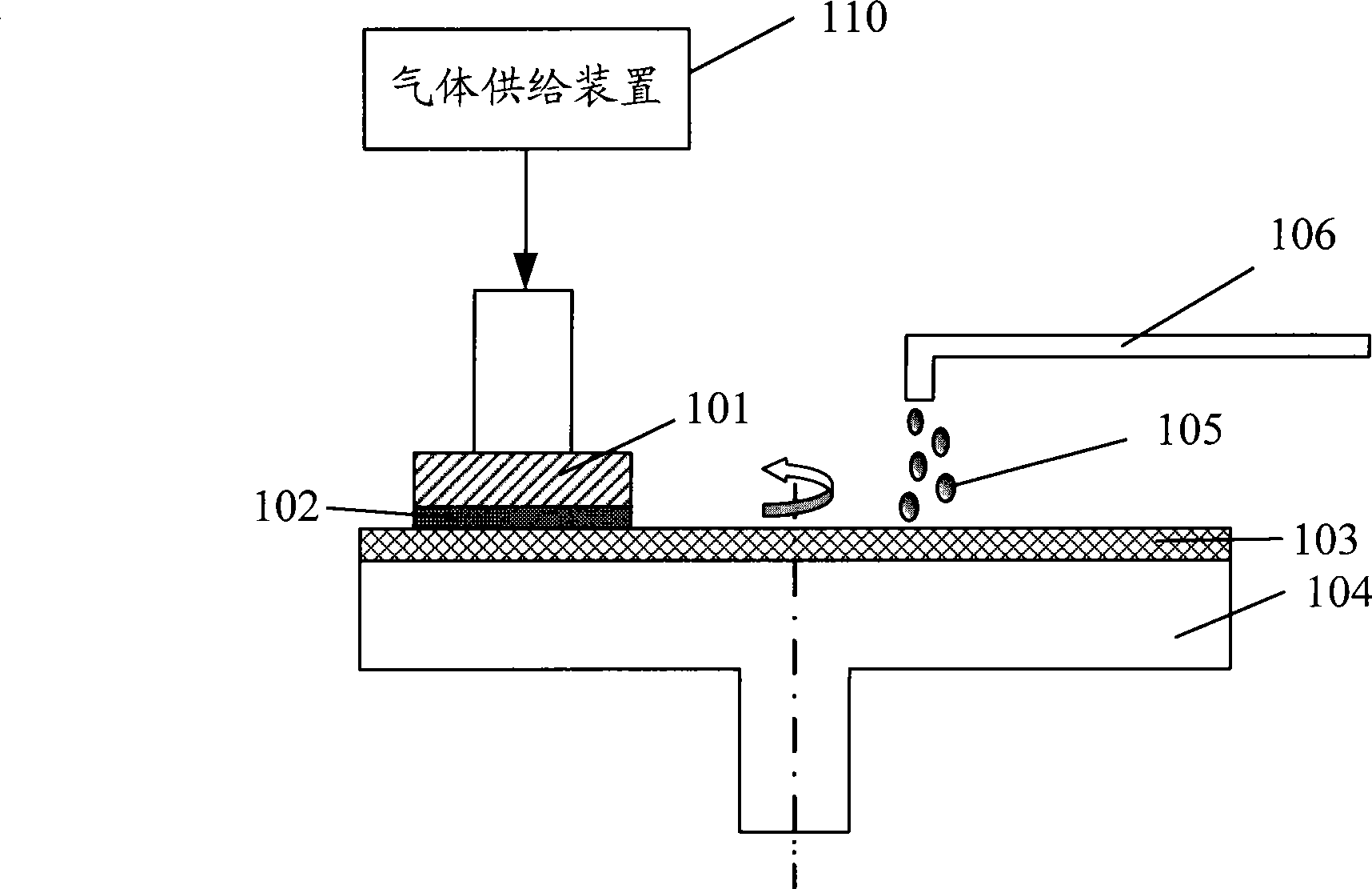
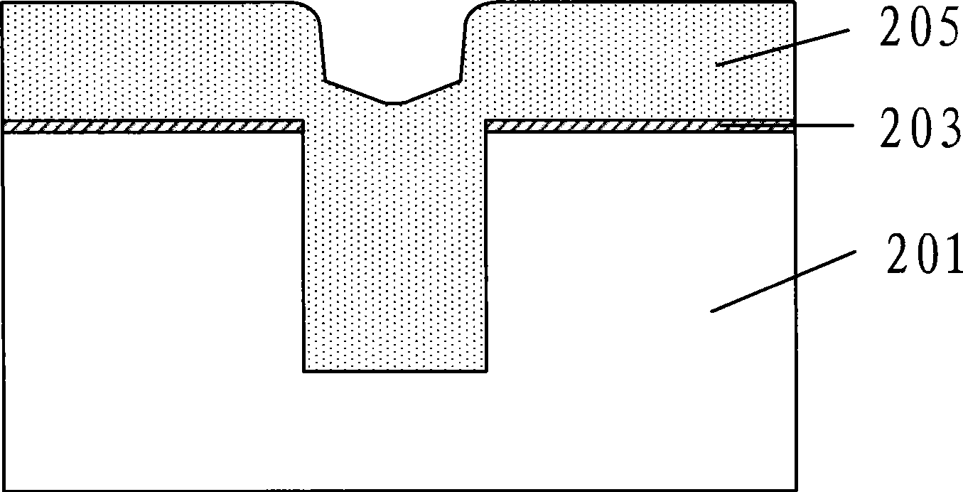
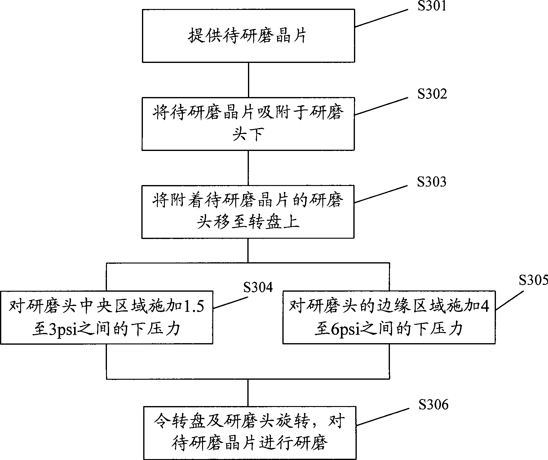
[0047] In order to make the above objects, features and advantages of the present invention more comprehensible, specific implementations of the present invention will be described in detail below in conjunction with the accompanying drawings.
[0048] The processing method of the present invention can be widely used in various fields, and can utilize many suitable materials to make, and the following is to illustrate by specific embodiment, certainly the present invention is not limited to this specific embodiment, in this field Common replacements known to those of ordinary skill undoubtedly fall within the protection scope of the present invention.
[0049] Secondly, the present invention has been described in detail using schematic diagrams. When describing the embodiments of the present invention in detail, for the convenience of explanation, the schematic diagrams showing the structure will not be partially enlarged according to the general scale, which should not be used...
PUM
 Abstract
Description
Claims
Application Information