Decision feedback equalizer of semiconductor storage device and initialization method thereof

A technology of decision feedback equalization and storage equipment, which is applied in the direction of static memory, electrical analog memory, digital memory information, etc., can solve the problems of failure to overcome delay, failure to compensate feedback delay, use restrictions, etc., to reduce operating frequency and reduce Errors, Effects of Resolving Usage Restrictions

Inactive Publication Date: 2009-05-06
SAMSUNG ELECTRONICS CO LTD
View PDF1 Cites 13 Cited by
  • Summary
  • Abstract
  • Description
  • Claims
  • Application Information

AI Technical Summary

Problems solved by technology

In addition, conventional DFE circuits may be limited in use due to their failure to compensate for feedback delays, resulting in an inability to overcome undesired delays

Method used


Image

  • Decision feedback equalizer of semiconductor storage device and initialization method thereof
  • Decision feedback equalizer of semiconductor storage device and initialization method thereof
  • Decision feedback equalizer of semiconductor storage device and initialization method thereof

Examples


Embodiment Construction

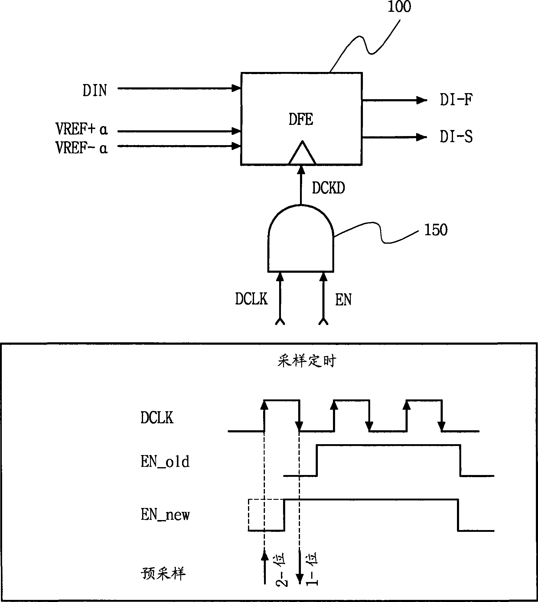
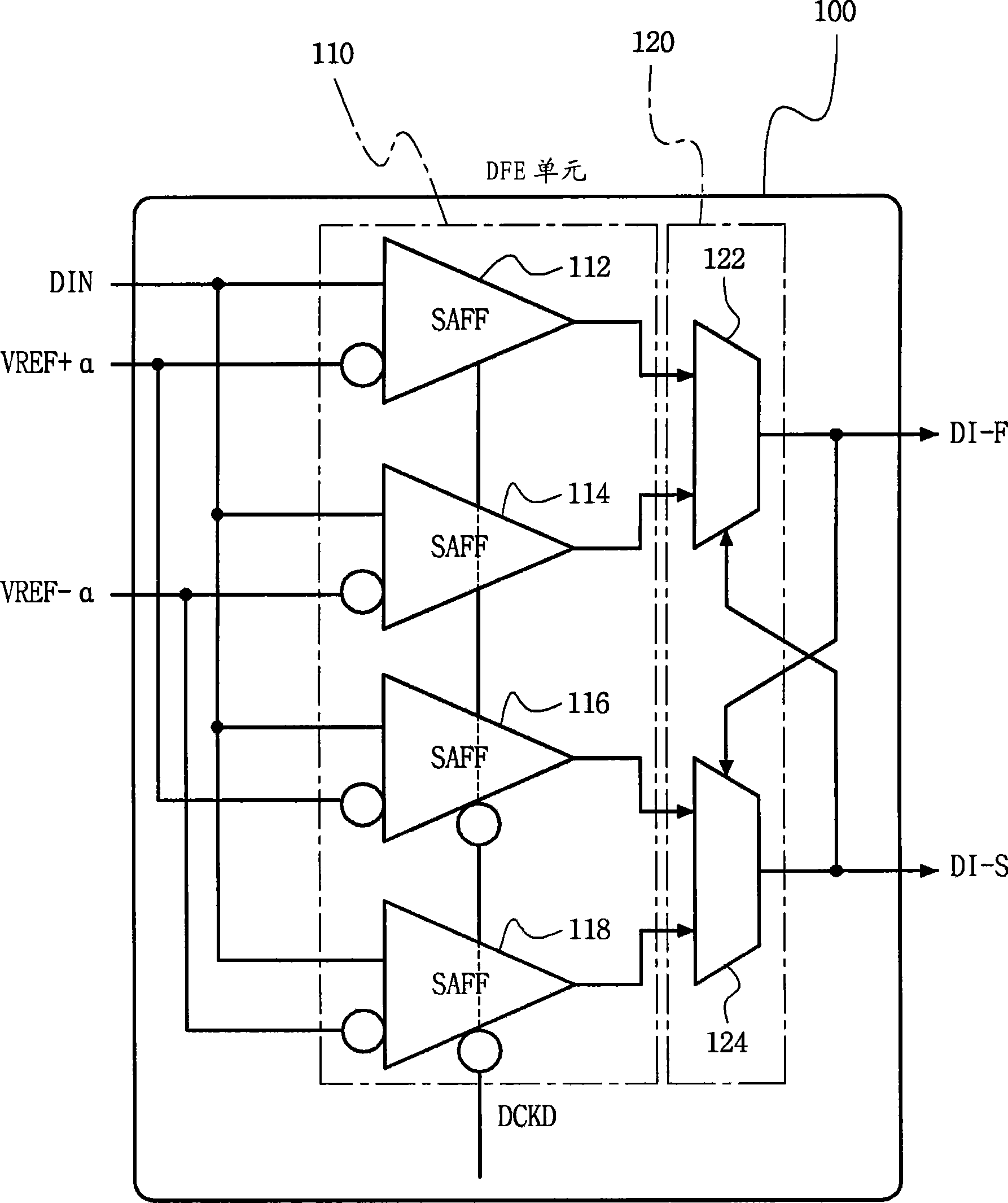
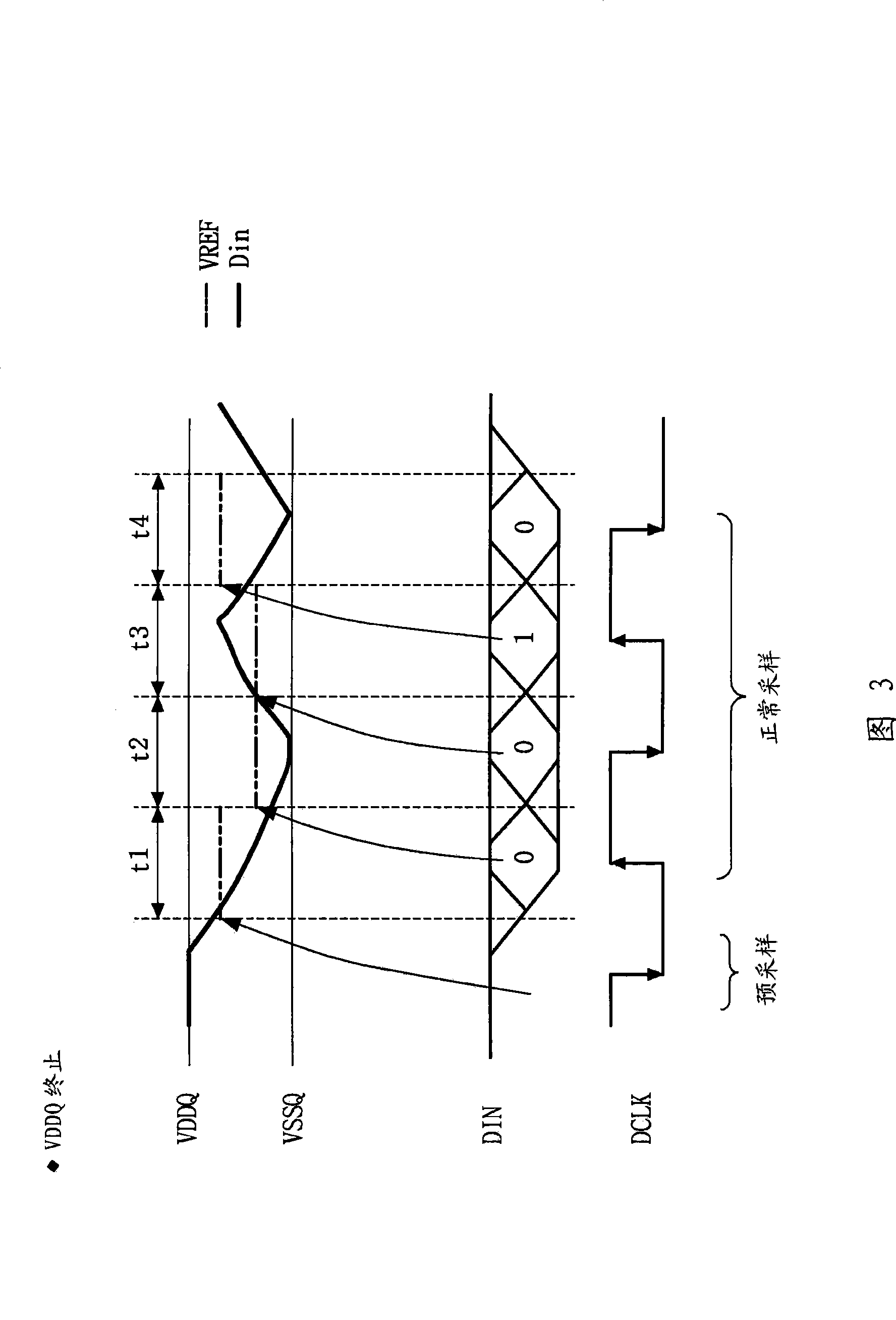
[0026] will now refer to figure 1 Turning to FIG. 8 , an embodiment of the present invention is described more fully below. However, this invention may be embodied in many different forms and should not be construed as limited to the embodiments set forth herein. Rather, these embodiments are provided so that this disclosure will be thorough and complete, and will fully convey the scope of the invention to those skilled in the art.

[0027] Unless otherwise defined, all terms (including technical and scientific terms) used herein have the same meaning as commonly understood by one of ordinary skill in the art to which this invention belongs. It will be further understood that the terms used herein should be interpreted in a meaning consistent with their meaning in the context of this specification and the relevant technical field, and will not be interpreted in an ideal or overly formal sense unless such definition is expressly provided herein. The following will refer to f...


PUM


Abstract

The present invention provides a DEF circuit which is used in a semiconductor storing device and an initiating method thereof. In the initiating method of DFE circuit in the semiconductor storing device which has discrete data transmission, the DFE circuit can be used for responding to the level of prior data and changing a sampling reference level and sampling the transmission data. The method comprises the steps of terminating a transmitted data channel with transmitted data at a preset position for terminating the level, and controlling the sampling starting time point of transmitted data as the time point which is prior to the transmission time point of transmitted data for a preset time. Furthermore, the data initialization can be executed based on the initial data which is obtained at the transmission starting time point through the pre-sampling of data channel thereby obtaining the initialization of DFE circuit and compensating the feedback delay.

Description

technical field [0001] The present invention relates to a semiconductor storage device, and more particularly, to a decision feedback equalizer (DFE) circuit for a semiconductor storage device and an initialization method thereof capable of initializing a DFE circuit in a semiconductor storage device with intermittent data transmission and capable of Compensate for feedback delays. Background technique [0002] Recent developments in the field of semiconductor technology have brought about increases in clock frequencies as well as increases in data transfer rates. In particular, the data rate between the memory and the memory controller is increasing, which causes distortion of the waveform of the data sent over the data channel. One reason for this is intersymbol interference (ISI). ISI is an effect where previous data has an impact on currently transmitted data due to data channel bandwidth limitations. [0003] In one widely used method for reducing the effect of ISI, ...

Claims


Application Information

Patent Timeline
Patent Type & Authority Applications(China)
IPC IPC(8): G11C7/10G11C7/22
CPCG11C7/1006G11C7/02G11C7/1084G11C7/20G11C7/1078G11C27/02G11C7/10G11C7/12
Inventor 金琼炫文龙三
Owner SAMSUNG ELECTRONICS CO LTD
Why Eureka
Try Eureka