Technique allowance-increasing contact hole layer layout method

A technology of process margin and contact hole, which is applied in special data processing applications, instruments, electrical digital data processing, etc., can solve the problems of reducing the photolithographic quality of the contact hole layer, reducing the process margin of the contact hole layer, and increasing the difficulty of the process, etc. , to achieve the effect of improving the process margin, increasing the process margin, and increasing the process window

Inactive Publication Date: 2010-08-25
SEMICON MFG INT (SHANGHAI) CORP +1
View PDF0 Cites 0 Cited by
  • Summary
  • Abstract
  • Description
  • Claims
  • Application Information

AI Technical Summary

Problems solved by technology

[0003] However, the process margin (Process Margin) of the isolated contact hole after adding scattering stripes is still small compared with the process margin of other non-isolated contact holes, so the isolated contact hole will reduce the process margin of the entire contact hole layer. , which increases the difficulty of the process and reduces the photolithography quality of the contact hole layer

Method used


Image

  • Technique allowance-increasing contact hole layer layout method
  • Technique allowance-increasing contact hole layer layout method
  • Technique allowance-increasing contact hole layer layout method

Examples


Embodiment Construction

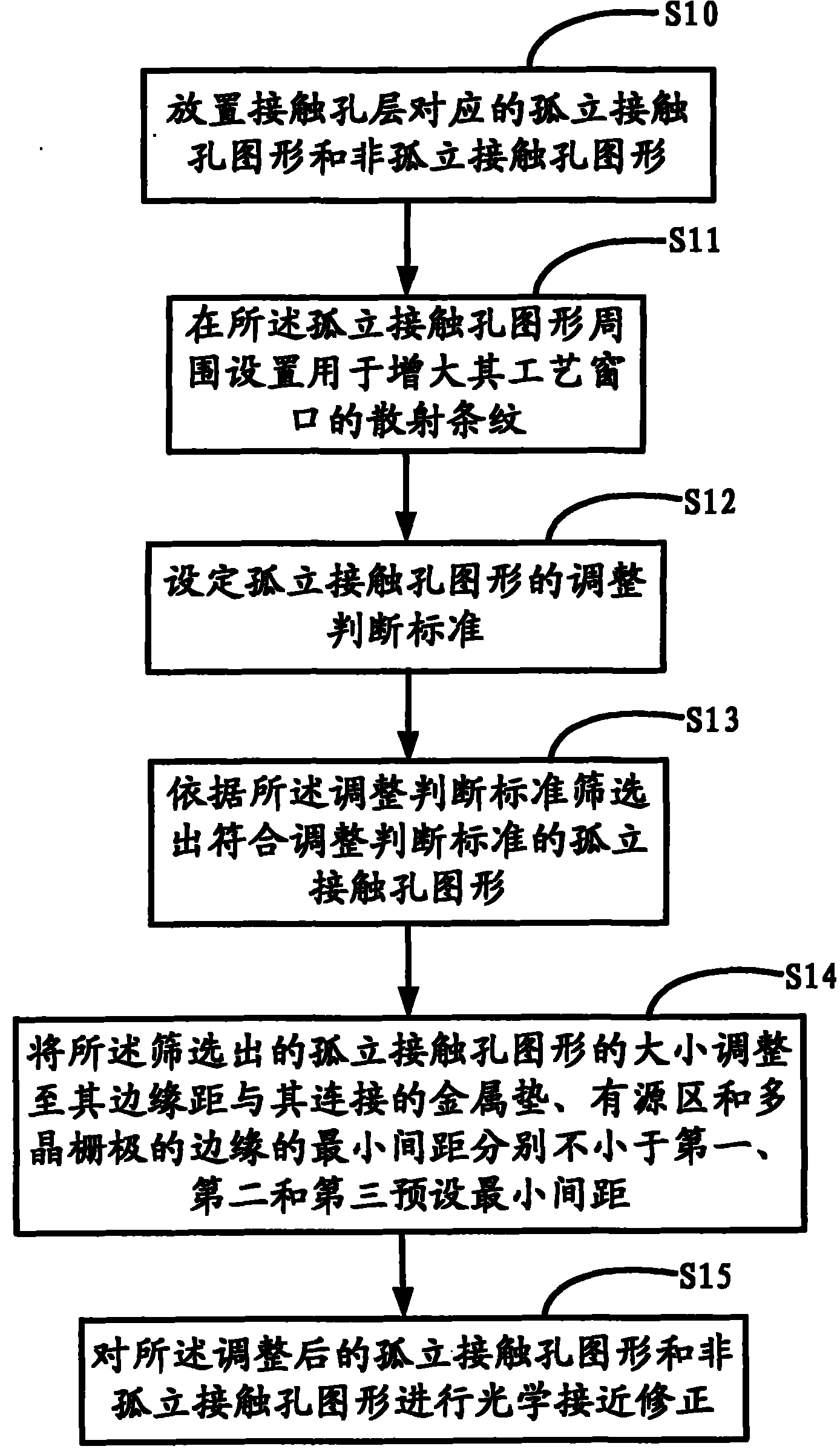
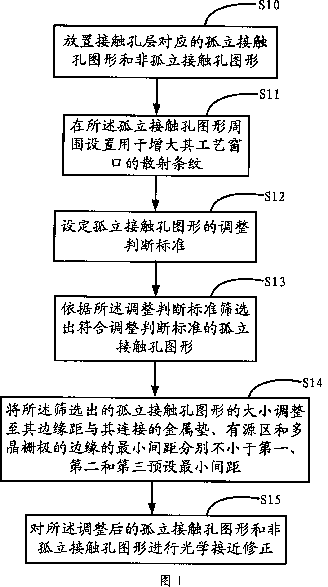
[0020] The contact hole layer patterning method that can increase the process margin of the present invention will be further described in detail below.

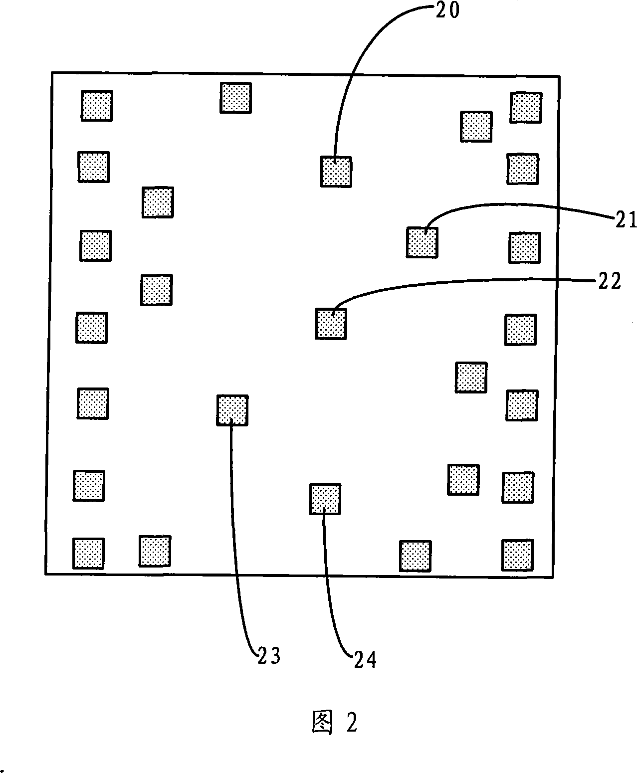
[0021] The contact hole layer layout method that can increase the process margin of the present invention is used for the layout layout of the contact hole layer by the user using the layout layout software. The contact hole layer has a plurality of metal pads, active An isolated contact hole and a non-isolated contact hole connecting the region and the polysilicon gate, the edge of the isolated contact hole is at least the first, the second and the second distance from the edge of the metal pad connected thereto, the active region and the polysilicon gate Three preset minimum spacing. In this embodiment, the layout software is L-Edit or Cadence layout software, the first, second and third preset minimum spacings are 50, 40 and 40 nanometers respectively, and the isolated contact Both the hole and the non-isolated contact h...


PUM


Abstract

The invention provides a method for laying out a contact hole layer which can increase process margin for a user to uses layout software for laying out the contact hole layer. The contact hole layer is provided with a plurality of isolated and nonisolated contact holes connected with a metal pad, an active area and a polycrystal grid; from edges of the isolated contact holes to edges of the metalpad, the active area and the polycrystal grid which are connected with the isolated contact holes, distances at least have first predetermined minimum spacing, second predetermined minimum spacing and third predetermined minimum spacing. The prior art can not overcome lower effect of the isolated contact holes to the process margin of the contact hole layer by setting scattered striation. The method for laying out the contact hole layer comprises the following steps: first, placing corresponding isolated and nonisolated contact hole patterns; then, setting the scattered striation; and then, setting an adjustment judging standard for the isolated contact hole patterns so as to screen an isolated contact hole pattern according with the adjustment judging standard, and adjusting the isolatedcontact hole pattern according to the first predetermined minimum spacing, the second predetermined minimum spacing and the third predetermined minimum spacing; finally, carrying out optical approaching correction. The method of the invention can increase the process margin.

Description

technical field [0001] The invention relates to the domain layout field, in particular to a contact hole layer layout method that can increase the process margin. Background technique [0002] In the field of semiconductor manufacturing, after the layout of the chip pattern of the semiconductor device is completed, it is necessary to convert the chip pattern into a layout that can be directly used for photomask manufacturing through layout layout, and then manufacture the photomask according to the laid out layout and perform photomask. Engraving process. With the continuous reduction of the minimum feature size (CD) of semiconductor devices (from the initial 1 mm to the current 90 nanometers or 60 nanometers, and will enter the era of 45 nanometers and 22 nanometers in the next few years), light The biggest challenge faced by the engraving process is how to maintain high image fidelity and process window under such a small CD, especially how to ensure image fidelity and pr...

Claims


Application Information

Patent Timeline
Patent Type & Authority Patents(China)
IPC IPC(8): G06F17/50
Inventor 王伟斌
Owner SEMICON MFG INT (SHANGHAI) CORP
Why Eureka
Try Eureka