Solution method of contact hole thick nitridation titanium film crack
A solution, the technology of titanium nitride, is applied in the direction of electrical components, semiconductor/solid-state device manufacturing, circuits, etc., and can solve problems such as cracks, side erosion, and affecting the quality of transistors.
- Summary
- Abstract
- Description
- Claims
- Application Information
AI Technical Summary
Problems solved by technology
Method used
Image

Examples
Embodiment Construction
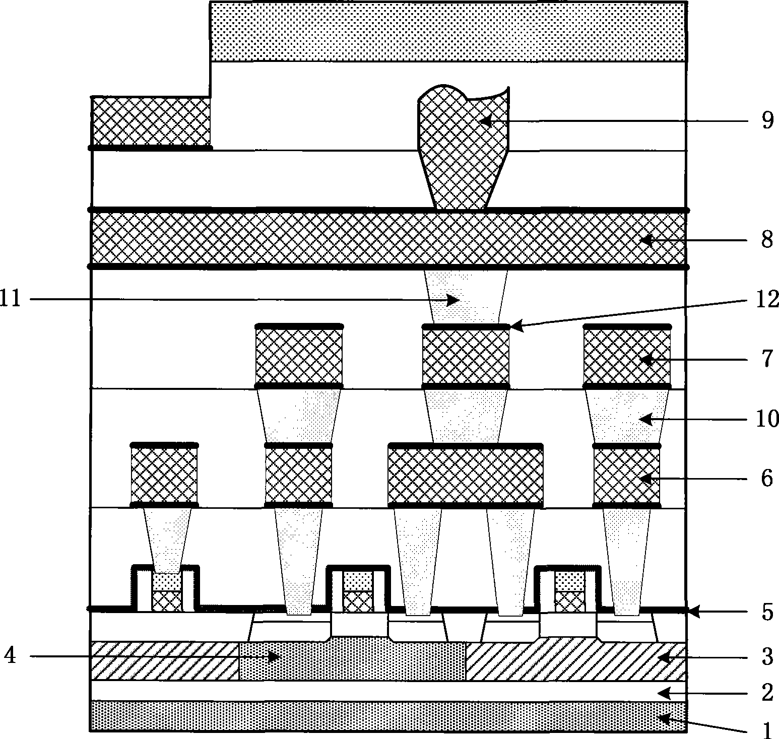
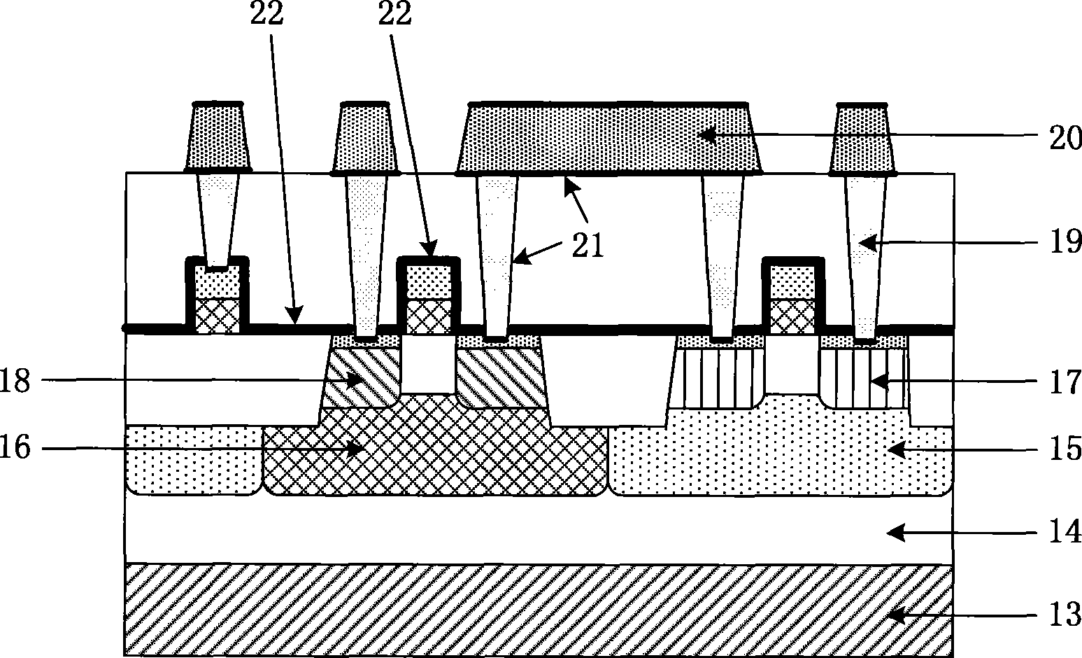
[0023] In order to enhance the adhesion between the deposited tungsten layer and the underlying metal layer, a layer of glue layer (Glue Layer) composed of titanium nitride (TiN) is usually formed before deposition. On the one hand, the function of the adhesive layer is to allow the deposited metal film to adhere to the substrate, and on the other hand, it will not affect the conduction of the deposited metal film.
[0024] The underside of the blanket tungsten deposit requires an adhesive layer first, otherwise the plated tungsten will flake off. Selective deposition directly fills metal tungsten into the contact window and dielectric window holes by chemical vapor deposition, reducing the manufacturing process, and the generated tungsten grows on the nucleation layer at the bottom of the contact window or dielectric window until it fills the entire hole without growing in the oxide dielectric above. There is no need to add an adhesion layer to the oxide surface, and no need...
PUM
 Abstract
Description
Claims
Application Information
 - R&D Engineer
- R&D Manager
- IP Professional
- Industry Leading Data Capabilities
- Powerful AI technology
- Patent DNA Extraction
Browse by: Latest US Patents, China's latest patents, Technical Efficacy Thesaurus, Application Domain, Technology Topic.
© 2024 PatSnap. All rights reserved.Legal|Privacy policy|Modern Slavery Act Transparency Statement|Sitemap