
Display apparatus and fabrication method and fabrication apparatus for the same

A technology for display devices and drive transistors, applied in static indicators, instruments, electrical components, etc., can solve problems such as characteristic fluctuations, luminous brightness effects, threshold voltage or mobility shifts, etc., to achieve high definition and reduce the number of components And the number of wiring, the effect of reducing the pixel array part

Inactive Publication Date: 2009-06-03
SONY CORP
View PDF2 Cites 13 Cited by
  • Summary
  • Abstract
  • Description
  • Claims
  • Application Information

AI Technical Summary

Problems solved by technology

[0014] However, the threshold voltage or mobility of active elements (i.e., drive transistors) used to drive electro-optical elements are shifted due to process fluctuations
In addition, the characteristics of electro-optic elements such as organic EL elements fluctuate over time
If there is such a shift in the characteristics of the driving active element or a fluctuation in the characteristics of the electro-optical element, this will have an effect on the luminance of light emission even when the constant current driving method is applied

Method used


Image

  • Display apparatus and fabrication method and fabrication apparatus for the same
  • Display apparatus and fabrication method and fabrication apparatus for the same
  • Display apparatus and fabrication method and fabrication apparatus for the same

Examples


Embodiment Construction

[0073] Hereinafter, embodiments of the present invention will be described with reference to the accompanying drawings.

[0074]

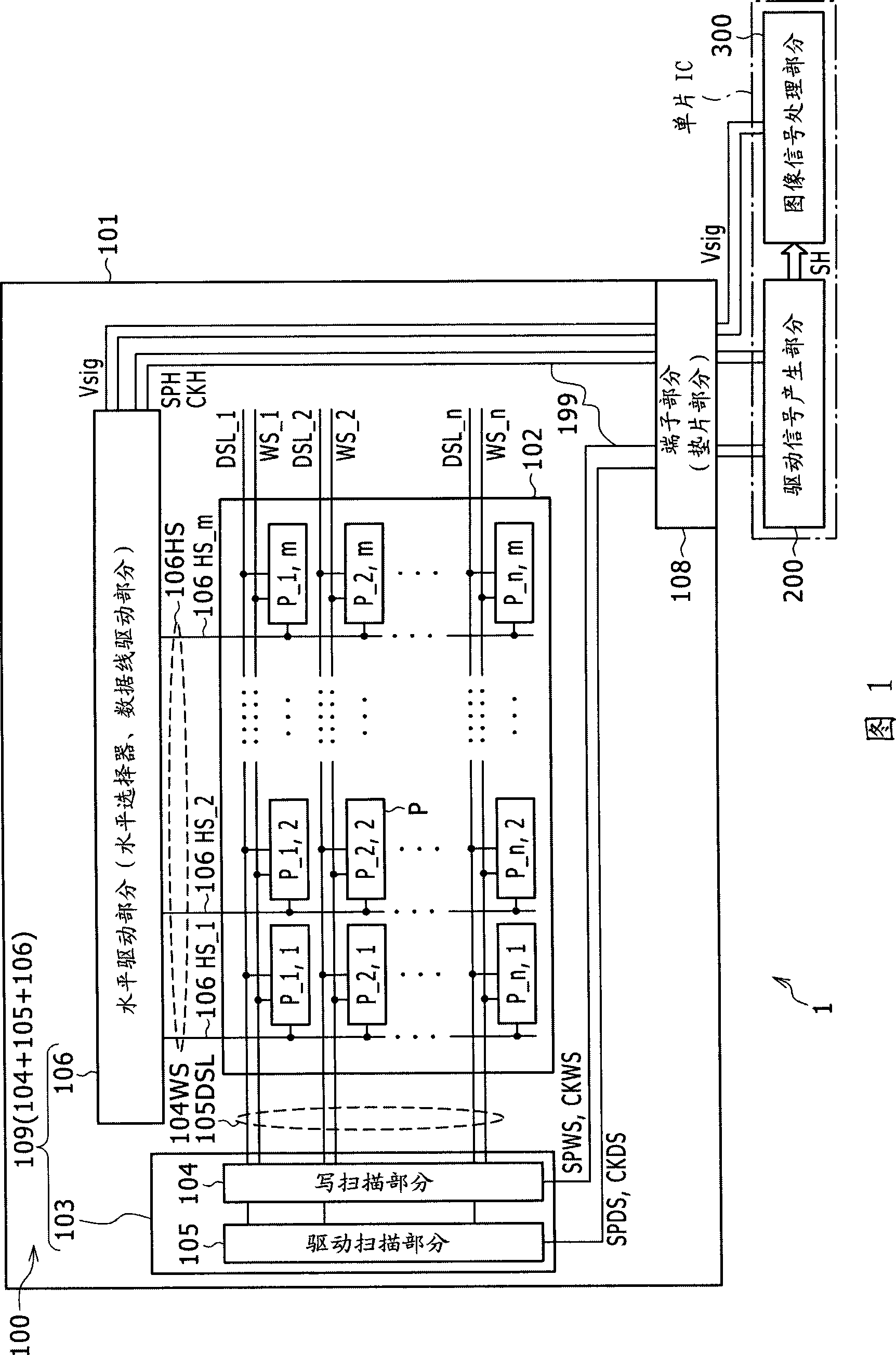
[0075] Referring first to FIG. 1 , shown is an example of the configuration of an active matrix display device as a display device according to a preferred embodiment of the present invention. In this embodiment, the present invention is applied to an active matrix organic EL display device (hereinafter simply referred to as "organic EL display device") in which, for example, an organic EL element and a polysilicon thin film transistor (TFT) are used as each The display element (electro-optic element or light-emitting element) and active element of a pixel. Furthermore, in an organic EL display device, such an organic EL element is formed on a semiconductor substrate on which a thin film transistor is formed.

[0076] It is to be noted that although an organic EL element is specifically described below as an example of a display element of a pix...


PUM


Abstract

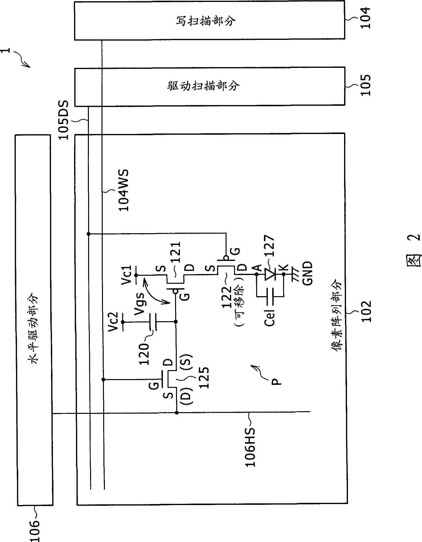
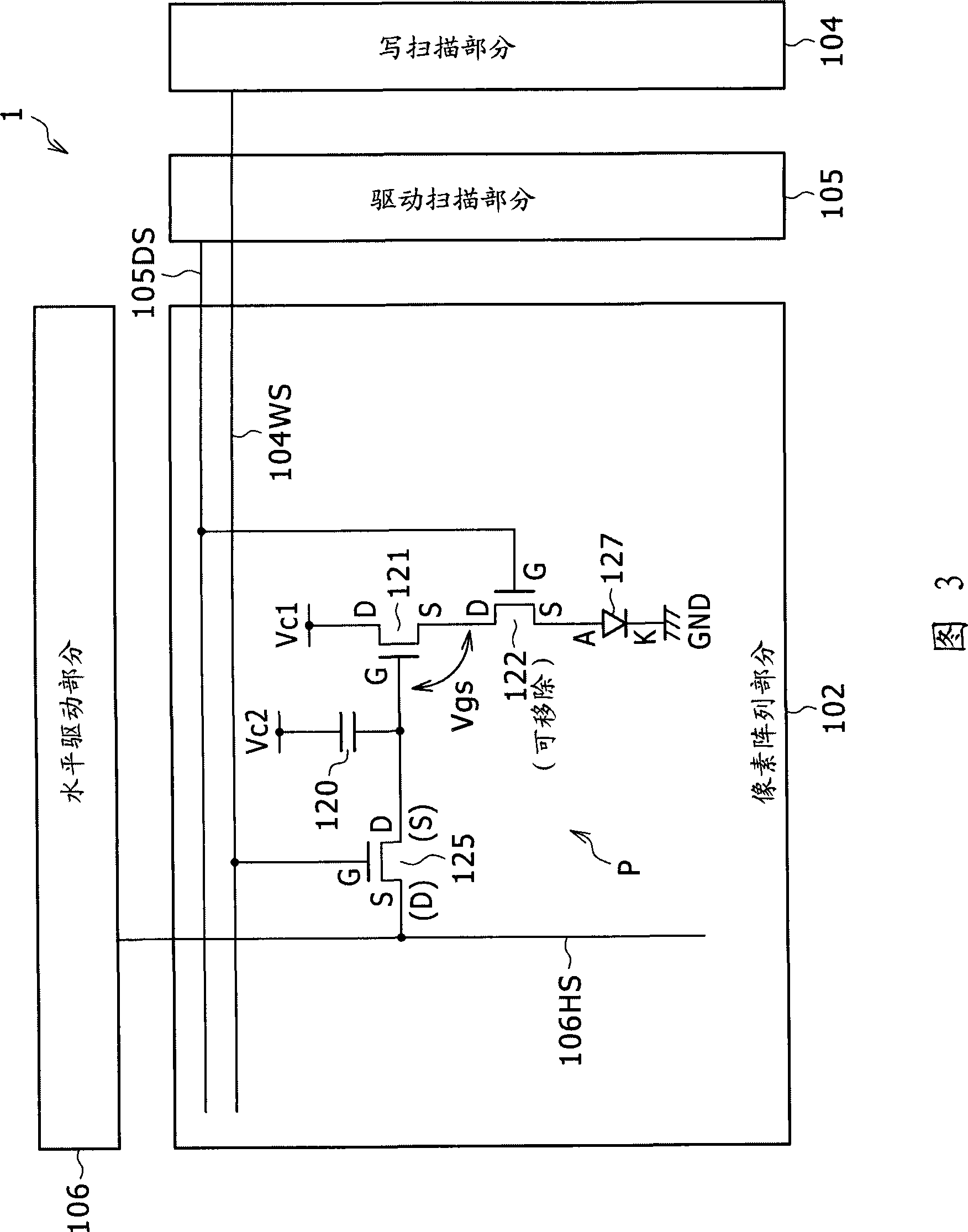
The invention discloses a display apparatus and fabrication method and fabrication apparatus for the same. The display apparatus includes: a pixel array section including a plurality of pixel circuits disposed in rows and columns and each including a driving transistor configured to produce driving current, a storage capacitor configured to store information in accordance with a signal amplitude of an image signal, an electro-optical element connected to an output terminal of the driving transistor, and a sampling transistor configured to write information in accordance with the signal amplitude into the storage capacitor, the driving transistor being operable to produce driving current based on the information stored in the storage capacitor and supply the driving current to the electro-optical element to cause the electro-optical element to emit light. The pixel circuit includes a pixel divided into a plurality of divisional pixels each of which independently includes the electro-optical element, the storage capacitor and the driving transistor.

Description

[0001] Cross References to Related Applications [0002] The present invention contains subject matter related to Japanese Patent Application JP2007-307860 filed in the Japan Patent Office on Nov. 28, 2007, the entire content of which is hereby incorporated by reference. technical field [0003] The present invention relates to a display device comprising a pixel array comprising a plurality of pixel circuits (hereinafter also referred to as pixels) arranged in rows and columns and each of which includes an electro-optic element (hereinafter also referred to as a display element or a light emitting element) part. More specifically, the present invention relates to an active matrix type display device in which a plurality of pixel circuits each including an electro-optic element whose luminance of light emission varies according to the current flowing therethrough are placed in rows and columns, and each pixel circuit The active elements included in the display drive are perfo...

Claims


Application Information

Patent Timeline
Patent Type & Authority Applications(China)
IPC IPC(8): G09G3/30G09G3/32
CPCG09G2320/045G09G2300/0842G09G2320/043G09G2300/0866G09G3/3233G09G2300/0819G09G3/3291H01L2027/11879H10K59/122
Inventor 内野胜秀山本哲郎
Owner SONY CORP
Learn More