Supercharge Your Innovation With Domain-Expert AI Agents!

Manufacturing method of double diffusion field effect transistor

A technology of field effect transistors and manufacturing methods, applied in semiconductor/solid-state device manufacturing, electrical components, circuits, etc., capable of solving large saturation current, rapid drop in device breakdown voltage, saturation current and breakdown voltage of double diffused field effect transistors It is difficult to optimize and other issues to achieve the effect of increasing the saturation current

Active Publication Date: 2010-05-26
SHANGHAI HUAHONG GRACE SEMICON MFG CORP
View PDF3 Cites 0 Cited by
  • Summary
  • Abstract
  • Description
  • Claims
  • Application Information

AI Technical Summary

Problems solved by technology

[0009] Due to the limitation of the above-mentioned method of manufacturing double-diffused transistors, it is difficult to obtain an optimal result between the saturation current and the breakdown voltage of the double-diffused field effect transistor (that is, to ensure a certain breakdown voltage, so that the saturation current reaches the maximum)
This is mainly because the doping distribution of the drift region does not have a certain concentration gradient change in the channel direction (that is, the lateral direction) of the transistor manufactured by the above-mentioned common process, specifically as figure 2 As shown, when the doping concentration of the drift region is increased in order to increase the saturation current, the breakdown voltage of the lateral abrupt junction in the drift region of the device will drop rapidly due to the increase of the doping concentration of the drift region, so that the breakdown of the entire device voltage drops rapidly

Method used


Image

  • Manufacturing method of double diffusion field effect transistor
  • Manufacturing method of double diffusion field effect transistor
  • Manufacturing method of double diffusion field effect transistor

Examples


Embodiment Construction

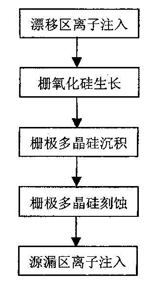
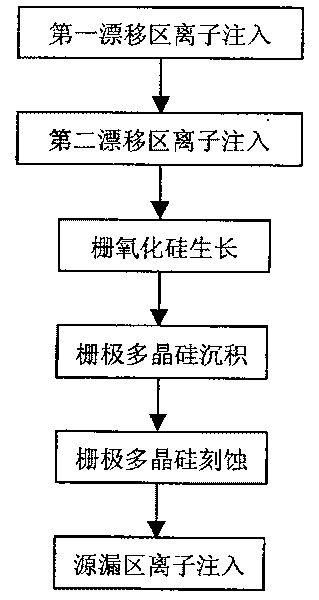
[0025] In one embodiment, such as image 3 Shown, method of the present invention comprises the following steps:

[0026] The first step is to carry out ion implantation on the silicon substrate to form a well region. Those skilled in the art should know that if the transistor to be manufactured is an N-type transistor, the ions to be implanted should be boron ions; The transistor to be manufactured is a P-type transistor, and the ions to be implanted at this time should be phosphorous ions.

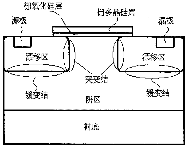
[0027] In the second step, the first selective ion implantation is performed at the position of the well region of the silicon substrate to form the first drift region, and the cross-sectional structure at this time is as follows Figure 4a shown. Those skilled in the art should know that if the transistor to be manufactured is an N-type transistor, the implanted ions should be phosphorus ions at this time; and if the transistor to be manufactured is a P-type transistor, the implanted ...


PUM


Abstract

The invention discloses a manufacturing method of a double diffusion field effect transistor, comprising the following steps: a drift region of the transistor can form a gradient slope with certain dosage concentration in a channel direction (namely in transverse direction) and a direction vertical to the channel direction (namely in longitudinal direction) by increasing one selective ions injection process for forming a second drift region, so that the junctions of the whole transistor in the transverse direction and longitudinal direction have approximately equal breakdown voltages and the transistor will not be broken down with small voltages; furthermore, the saturation currents of the transistor can be increased by increasing the dosage concentration at the drift region with certain breakdown voltages.

Description

technical field [0001] The invention relates to semiconductor process technology, in particular to a method for manufacturing a double-diffusion field effect transistor. Background technique [0002] For the existing semiconductor process technology, double diffused field effect transistor (Double Diffuse Drain MOS, DDDMOS for short) is a mainstream high-voltage device structure, which is widely used in driver chips and power devices. [0003] Such as figure 1 As shown, in the prior art, the double-diffused transistor is generally manufactured according to the following method: [0004] Firstly, performing ion implantation on the silicon substrate to form a well region, and then performing selective ion implantation in the well region to form a drift region; [0005] Then, growing a gate silicon oxide layer on the well region; [0006] The third step is to deposit a gate polysilicon layer on the gate silicon oxide layer; [0007] The fourth step is to use known photolith...

Claims


Application Information

Patent Timeline
Patent Type & Authority Patents(China)
IPC IPC(8): H01L21/336H01L21/265
Inventor 钱文生刘俊文
Owner SHANGHAI HUAHONG GRACE SEMICON MFG CORP
Features
  • R&D
  • Intellectual Property
  • Life Sciences
  • Materials
  • Tech Scout
  • Unparalleled Data Quality
  • Higher Quality Content
  • 60% Fewer Hallucinations
Learn More