Gallium oxide vertical structure semiconductor electronic device and manufacturing method thereof

A vertical structure and electronic device technology, applied in semiconductor devices, semiconductor/solid-state device manufacturing, electrical components, etc., can solve problems such as large breakdown voltage, lower production costs, buffer layer leakage, etc., achieve large saturation current, simple structure , the effect of high breakdown voltage

Inactive Publication Date: 2019-12-31
SUZHOU INST OF NANO TECH & NANO BIONICS CHINESE ACEDEMY OF SCI
View PDF6 Cites 5 Cited by
  • Summary
  • Abstract
  • Description
  • Claims
  • Application Information

AI Technical Summary

Problems solved by technology

However, the horizontal device has the following disadvantages compared with the vertical device: when the horizontal structure electronic device is in the off state, electrons can reach the drain terminal from the semi-insulating buffer layer, forming a leakage phenomenon of the buffer layer, and serious leakage of the buffer layer will make the drain end The pole current has reached the condition for breakdown judgment at a lower voltage
At the same time, electronic devices with a horizontal structure mainly rely on the active region between the gate and the drain to withstand the withstand voltage. To obtain a large breakdown voltage, it is necessary to design a large distance between the gate and the drain, thereby increasing the size of the chip. The required area does not meet the needs of miniaturization, and it is not conducive to reducing the production cost
High-power conversion applications require high current and high voltage, and chips designed with horizontal structures are not economical and difficult to fabricate
[0006] In addition, in the horizontal device, the high electric field region is located at the edge of the gate near the drain side, because the high electric field injects electrons into the traps existing on the surface, causing the collapse of the current. This serious reliability problem further limits the horizontal device. Applications in the field of high pressure

Method used


Image

  • Gallium oxide vertical structure semiconductor electronic device and manufacturing method thereof

Examples


Embodiment Construction

[0018] In view of the deficiencies in the prior art, the inventor of this case was able to propose the technical solution of the present invention after long-term research and extensive practice. The technical solution, its implementation process and principle will be further explained as follows.

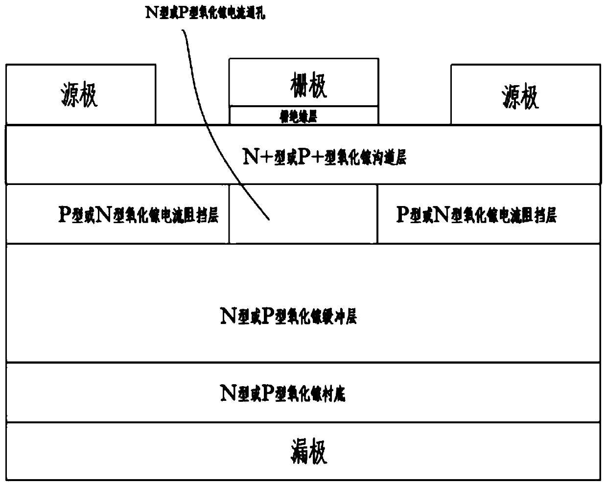
[0019] An embodiment of the present invention provides a semiconductor electronic device with a gallium oxide vertical structure, which includes a buffer layer, a current blocking layer, and a channel layer arranged in sequence, and the current blocking layer is also distributed with current formed by ion implantation. A through hole, the channel layer is provided with a source and a gate, the buffer layer is connected to the drain, the drain is arranged opposite to the current blocking layer, and the current through hole is located under the gate, so The channel layer is electrically connected to the buffer layer through the current via hole.

[0020] Further, when the device is ...


PUM

PropertyMeasurementUnit
Thicknessaaaaaaaaaa

Abstract

The invention discloses a gallium oxide vertical structure semiconductor electronic device and a preparation method thereof. The gallium oxide vertical structure semiconductor electronic device comprises a buffer layer, a current blocking layer and a channel layer which are arranged in sequence, wherein current through holes formed through ion implantation processing are further distributed in thecurrent blocking layer; a source electrode and a gate electrode are arranged on the channel layer; the buffer layer is connected with a drain electrode; the drain electrode and the current blocking layer are arranged back to back; the current through holes are located below the gate electrode; and the channel layer is electrically connected with the buffer layer through the current through holes.The gallium oxide vertical structure semiconductor electronic device provided in the invention is simple in structure, can well meet the requirements of a high-power switch, has a series of advantages of large saturation current, high breakdown voltage and the like, greatly exerts the characteristics of a Ga2O3 material, and plays a greater role in the field of power semiconductor electronic devices.

Description

technical field [0001] The invention particularly relates to a gallium oxide vertical structure semiconductor electronic device and a manufacturing method thereof, belonging to the technical field of semiconductor devices. Background technique [0002] In modern society, power electronic technology is the core to realize the conversion and utilization of various energy and electric energy, and also the foundation and important pillar of national economy and national security. Power electronic devices play a decisive role in the application and market of power electronic technology. Function, it is a bridge between weak current control and strong current operation, and is the basic support for information technology and advanced manufacturing technology, traditional and modern industries to realize automation, intelligence, energy saving, and mechatronics. With the continuous development of wireless technologies such as high-voltage frequency conversion, AC drive locomotives / ...

Claims


Application Information

Patent Timeline
IPC IPC(8): H01L29/78H01L29/24H01L21/34
CPCH01L29/24H01L29/66969H01L29/7828H01L21/34H01L29/778H01L29/78
Inventor 张晓东李军帅张丽邓旭光范亚明张宝顺
Owner SUZHOU INST OF NANO TECH & NANO BIONICS CHINESE ACEDEMY OF SCI
Why Eureka
Try Eureka