Inversed LED (Light Emitting Diode) chip structure and preparation method of inversed LED chip

A LED chip and flip-chip technology, applied in the direction of electrical components, circuits, semiconductor devices, etc., can solve the problems of poor chip reliability, making electrode patterns, and reduced light efficiency, so as to achieve improved performance, good support, and increased reliability. Effect

Inactive Publication Date: 2012-09-19
HANGZHOU SILAN AZURE
View PDF4 Cites 5 Cited by
  • Summary
  • Abstract
  • Description
  • Claims
  • Application Information

AI Technical Summary

Problems solved by technology

Moreover, the expansion of the metal substrate will split the GaN lattice with low tensile strength, generate defects inside the lattice, cause local heating in the epitaxial layer, and lead to a vicious circle of reduced light efficiency. Such chips have poor reliability; A large difference in expansion coefficient will cause a certain degree of curvature on the upper and lower sides of the wafer, so that the subsequent pattern photolithography process cannot make electrode patterns well, and it is easy to cause pattern offset and deformation

Method used


Image

  • Inversed LED (Light Emitting Diode) chip structure and preparation method of inversed LED chip
  • Inversed LED (Light Emitting Diode) chip structure and preparation method of inversed LED chip
  • Inversed LED (Light Emitting Diode) chip structure and preparation method of inversed LED chip

Examples


Embodiment 1

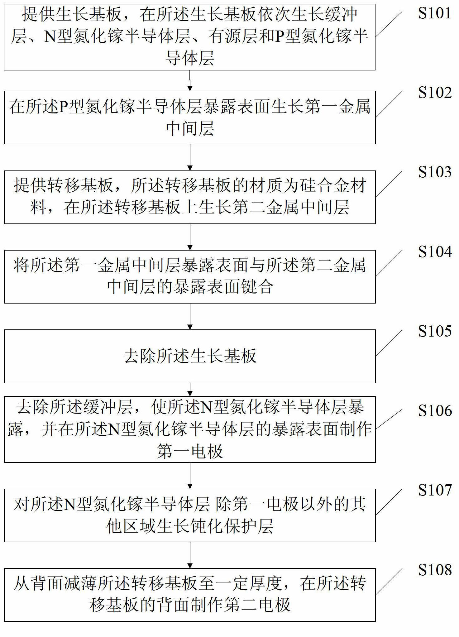
[0092] On the growth substrate made of sapphire, a buffer layer made of GaN, an N-type semiconductor layer made of GaN, an active layer made of InGaN and a P-type semiconductor layer made of GaN are sequentially deposited by metal-organic chemical vapor deposition;

[0093] Depositing a first metal intermediate layer composed of Ni / Ag / Ti / W / Au / Sn elements on the surface of the P-type semiconductor layer made of GaN;

[0094] A second metal interlayer made of Au / Sn elements is deposited on a silicon alloy transfer substrate with a silicon content of 80 wt % and an aluminum content of 20 wt %. The silicon alloy material with a silicon content of 80wt% and an aluminum content of 20wt% has a thermal expansion coefficient similar to that of sapphire;

[0095] The first metal intermediate layer and the second metal intermediate layer are bonded in a vacuum thermocompression in opposite directions, so that the first metal intermediate layer and the second metal intermediate layer diff...

Embodiment 2

[0109]On the growth substrate made of sapphire, a buffer layer made of GaN, an N-type semiconductor layer made of GaN, an active layer made of InGaN and a P-type semiconductor layer made of GaN are sequentially deposited by metal-organic chemical vapor deposition;

[0110] Depositing a first metal intermediate layer made of Ag / Ti / Au / Sn elements on the surface of the P-type semiconductor layer made of GaN;

[0111] A second metal interlayer made of Au / Sn elements is deposited on a silicon alloy transfer substrate with a silicon content of 50 wt%, an aluminum content of 40 wt%, and a copper content of 10 wt%.

[0112] The first metal intermediate layer and the second metal intermediate layer are bonded in a vacuum thermocompression in opposite directions, so that the first metal intermediate layer and the second metal intermediate layer diffuse each other to form a metal alloy. The parameters of vacuum thermocompression bonding include: the gas pressure is 1torr, the temperature...


PUM


Abstract

The invention provides an inversed LED (Light Emitting Diode) chip structure which comprises a silicon alloy substrate, a metal middle layer, a P-type gallium nitride semiconductor layer, an active layer and a N-type gallium nitride semiconductor layer sequentially stacked from bottom to top. According to the inversed LED chip structure, a transfer substrate made of silicon alloy which is approximate to a growth substrate in thermal expansion coefficient is adopted as the substrate of the LED chip to reduce the staggered damage of lattices of an LED chip apparatus layer, therefore, the leakage current is reduced, and the performance of product is improved. The invention further provides a preparation method of the inversed LED chip structure.

Description

technical field [0001] The invention relates to a flip-chip LED chip structure and a preparation method thereof, and belongs to the technical field of semiconductor manufacturing. Background technique [0002] With the frequent occurrence of extreme climates around the world, the field of lighting is also entering a major revolution. As the third-generation solid-state lighting technology, LED is being highly concerned by everyone; but with the development of technology, the mature existing technology is facing huge challenges. At present, the most mature method is to grow the gallium nitride crystal layer on the sapphire insulating substrate, so the positive and negative electrodes are made on the same side, and the light is emitted from the p-side gallium nitride layer to the environment; in this structure, the current will flow laterally The N-type gallium nitride layer leads to current crowding and local heating, which reduces the electro-optical conversion efficiency; ...

Claims


Application Information

Patent Timeline
Patent Type & Authority Applications(China)
IPC IPC(8): H01L33/02H01L33/12H01L33/00
Inventor 张昊翔金豫浙封飞飞万远涛高耀辉李东昇江忠永
Owner HANGZHOU SILAN AZURE
Why Eureka
Try Eureka