Metal oxide semiconductor field effect transistor

An oxide semiconductor and field effect transistor technology, applied in the field of metal oxide semiconductor field effect transistors, can solve the problems of increased threshold voltage, reduced device saturation current, poor gate-to-channel control capability, etc. Effects of leakage current, increased saturation current, and improved drive capability

Active Publication Date: 2009-06-03
SHANGHAI HUAHONG GRACE SEMICON MFG CORP
View PDF0 Cites 5 Cited by
  • Summary
  • Abstract
  • Description
  • Claims
  • Application Information

AI Technical Summary

Problems solved by technology

However, this method has obvious disadvantages, that is, when the thickness of the gate insulating dielectric layer of the MOSFET becomes larger, the control ability of the gate to the channel becomes worse, and the threshold voltage increases, resulting in a decrease in the saturation current of the device.

Method used


Image

  • Metal oxide semiconductor field effect transistor
  • Metal oxide semiconductor field effect transistor
  • Metal oxide semiconductor field effect transistor

Examples


Embodiment Construction

[0022] In order to understand the technical content of the present invention more clearly, specific embodiments are given and described as follows in conjunction with the accompanying drawings.

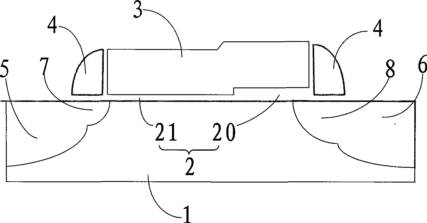
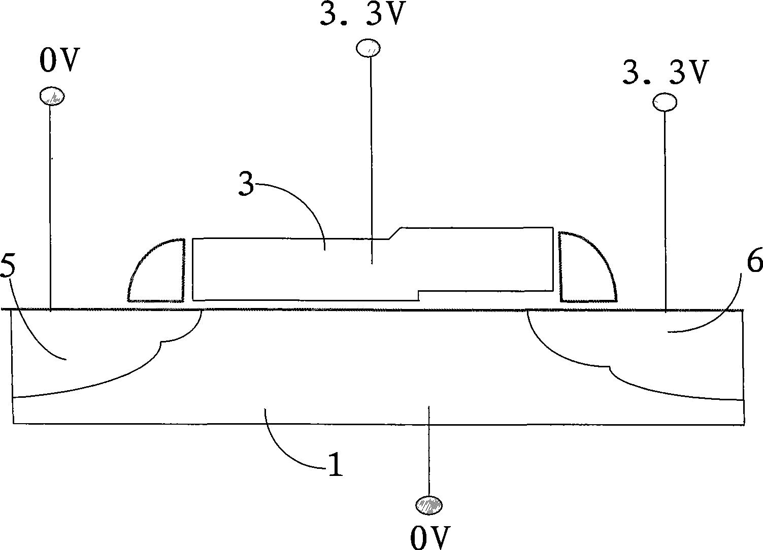
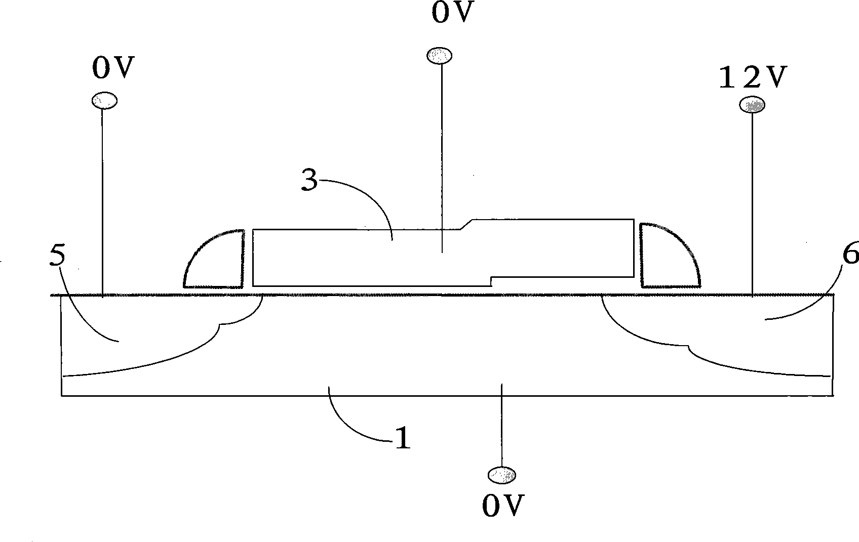
[0023] see figure 1 , figure 1 It is a schematic structural diagram of a metal oxide semiconductor field effect transistor in an embodiment of the present invention, the metal oxide semiconductor field effect transistor includes a semiconductor substrate 1, and a gate insulating dielectric layer 2 is arranged on the surface of the semiconductor substrate 1, The gate insulating dielectric layer 2 is silicon oxide, silicon oxynitride, HfO2 or other dielectric layers with high dielectric constants. In this embodiment, the gate insulating dielectric layer 2 is silicon oxide Silica.

[0024] The gate 3 is stacked on the upper surface of the gate insulating dielectric layer 2, and the gate 3 is a polysilicon gate. A gate spacer 4 is provided on the upper surface of the gate insulating di...


PUM

PropertyMeasurementUnit
Thicknessaaaaaaaaaa
Thicknessaaaaaaaaaa

Abstract

The invention discloses a metal oxide semiconductor field effect transistor which comprises a semiconductor substrate, a grid insulation dielectric layer which is arranged on the surface of the semiconductor substrate, a grid which is piled on the grid insulation dielectric layer and a source electrode area and a drain electrode area which are arranged in the surface area of the semiconductor substrate at two sides of the grid and are separated by a channel region. A first part of the grid insulation dielectric layer is close to the drain electrode area, a second part thereof is close to the source electrode area, and the thickness of the first part is thicker than the thickness of the second part. The thickness of the second part near the source electrode area of the metal oxide semiconductor field effect transistor is thinner, thereby improving the control capacity of the grid on the channel, increasing saturation current, improving the drive capacity of the apparatus and also reducing the area of the apparatus. The thickness of the first part near the drain electrode area is thicker, thereby controlling leakage current caused by GIDL effect.

Description

technical field [0001] The invention relates to a semiconductor device, in particular to a metal oxide semiconductor field effect transistor. Background technique [0002] The application environment of metal-oxide-semiconductor field-effect transistors (MOSFETs) is increasingly complex and needs to work under different voltage conditions. For example, in memory peripheral circuits, it is often necessary for a MOSFET drain to withstand a higher voltage in the "off" state. Voltage (such as 12V), while in the "on" state, the gate and drain only bear the normal operating voltage (such as 3.3V). When a high voltage is applied to the drain, due to the gate-induced-drain leakage (GIDL) effect, the drain will generate a large leakage current, which will increase the power consumption of the device and affect the working life of the device. [0003] The magnitude of the leakage current caused by the GIDL effect is directly related to the thickness of the gate insulating dielectric ...

Claims


Application Information

Patent Timeline
IPC IPC(8): H01L29/78H01L29/423
Inventor 孔蔚然
Owner SHANGHAI HUAHONG GRACE SEMICON MFG CORP
Why Eureka
Try Eureka