High-voltage-resistant bigrid transverse HEMT device and preparation method thereof

A double gate, high withstand voltage technology, applied in the field of HEMT devices, can solve problems such as device breakdown

Active Publication Date: 2021-07-13
SOUTH CHINA NORMAL UNIVERSITY
View PDF12 Cites 5 Cited by
  • Summary
  • Abstract
  • Description
  • Claims
  • Application Information

AI Technical Summary

Problems solved by technology

In the off state, electrons injected from the source pass through the buffer layer to the drain to form a current channel, causing premature breakdown of the device

Method used


Image

  • High-voltage-resistant bigrid transverse HEMT device and preparation method thereof
  • High-voltage-resistant bigrid transverse HEMT device and preparation method thereof
  • High-voltage-resistant bigrid transverse HEMT device and preparation method thereof

Examples


Embodiment Construction

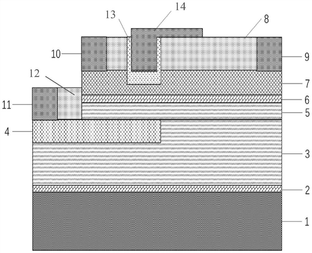
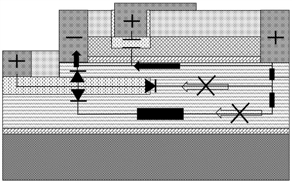
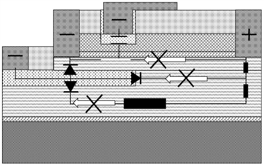
[0034] Next, the technical solutions in the embodiments of the present invention will be clearly and completely described in conjunction with the accompanying drawings of the present invention, and the described embodiments are only some of the embodiments of the present invention, not all of them. Based on the embodiments in the present invention, structural or logical changes may be made without departing from the scope of the present invention. The scope of the invention is defined by the appended claims.

[0035] Spatially relative terms such as "under", "beneath", "under", "above", "above", "on" are used in this specification to explain the positioning of one element relative to a second element. These terms are intended to encompass different orientations of the device in addition to orientations other than those depicted in the figures.

[0036] In addition, the use of terms such as "first", "second", etc. to describe various elements, regions, sections, etc., is not i...


PUM

PropertyMeasurementUnit
thicknessaaaaaaaaaa
lengthaaaaaaaaaa
thicknessaaaaaaaaaa

Abstract

The invention relates to a high-voltage-resistant bigrid transverse HEMT device, which comprises a buffer layer positioned on a substrate, and a laminated layer consisting of a GaN channel layer, an AlN insertion layer and an AlGaN barrier layer which are sequentially laminated on the buffer layer, and also comprises a p-type buried layer, a grid positioned on the p-type buried layer, and a source / drain electrode and an inverted L-shaped grid which are positioned on the barrier layer; in the thickness direction, the p-type buried layer extends by a certain depth from the surface, close to the channel layer, of the buffer layer to the side, away from the channel layer, of the buffer layer; the source and the drain are located on the surface of the barrier layer; a gate groove is formed between the source electrode and the drain electrode, and the inverted L-shaped gate is located in the gate groove and extends towards one side of the drain electrode; and in the length direction, the p-type buried layer extends from the position below the grid electrode to the position below the grid groove. Through the introduction of the p-type buried layer and the structural arrangement of double gates combined with the AlGaN / AlN / GaN heterojunction, the HEMT device with low on-resistance, high saturation current, high breakdown voltage and low leakage current is obtained.

Description

technical field [0001] The invention relates to the technical field of HEMT devices, in particular to a high withstand voltage double-gate lateral HEMT device and a preparation method thereof. Background technique [0002] AlGaN / GaN HEMT devices have surpassed Si-based power devices in terms of high power, high operating temperature, and strong radiation resistance. They not only have the advantages of GaN materials, but also AlGaN / GaN heterojunctions. Polarized electric fields, capable of forming a two-dimensional electron gas (2DEG) with high mobility and high carrier areal density, have received great attention in the field of power electronics. [0003] Although AlGaN / GaN HEMT devices have high withstand voltage characteristics in theory, the breakdown voltage of actual devices is only a few hundred volts, which is still far from the theoretical withstand voltage limit of GaN materials, which limits the development of GaN-based HEMT devices. large-scale application. Th...

Claims


Application Information

Patent Timeline
Patent Type & Authority Applications(China)
IPC IPC(8): H01L29/06H01L29/423H01L29/778H01L21/28H01L21/335
CPCH01L29/7787H01L29/66462H01L29/0684H01L29/0623H01L29/401H01L29/42356H01L29/4236H01L29/0638H01L29/0665Y02P70/50H01L29/7786H01L29/2003H01L29/402H01L29/0657
Inventor 尹以安李佳霖
Owner SOUTH CHINA NORMAL UNIVERSITY
Why Eureka
Try Eureka