

Radio-frequency LDMOS (Laterally Diffused Metal Oxide Semiconductor) device and manufacturing method thereof
A device and radio frequency technology, which is applied in the field of semiconductor integrated circuit manufacturing, can solve the problems that the drift region 4 cannot be fully depleted, the breakdown voltage increases, the drift region decreases, etc., and achieves the reduction of hot carrier injection capability, increase of drive current, Effect of Reducing On-Resistance
- Summary
- Abstract
- Description
- Claims
- Application Information
AI Technical Summary
Problems solved by technology
Method used
Image

Examples
Embodiment Construction
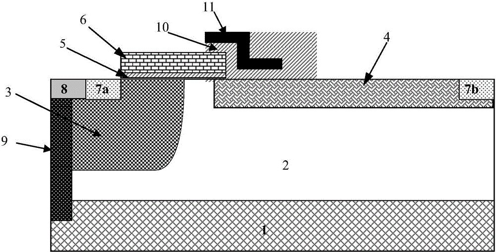
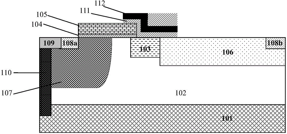
[0050] Such as figure 2 As shown, it is a schematic structural diagram of the radio frequency LDMOS device of the embodiment of the present invention; the radio frequency LDMOS device of the embodiment of the present invention is described by taking an N-type device as an example, and the radio frequency LDMOS device of the embodiment of the present invention includes:
[0051] P-type heavily doped silicon substrate 101 . The doping concentration of the silicon substrate 1 is greater than 1e20cm -3 .
[0052] A P-type doped silicon epitaxial layer 102 , the silicon epitaxial layer 102 is formed on the surface of the silicon substrate 101 . The doping concentration range of the silicon epitaxial layer 2 is 1×10 14 cm -3 to 1×10 16 cm -3 , with a thickness of 1 μm to 10 μm.
[0053] A polysilicon gate 5 , a gate dielectric layer 4 is separated between the polysilicon gate 5 and the silicon epitaxial layer 102 , and the polysilicon gate 5 is formed by photoetching and etc...
PUM
 Abstract
Description
Claims
Application Information