Production of layout and photo mask and graphic method

A technology of layout method and manufacturing method, which is applied to the original parts, optics, and opto-mechanical equipment for opto-mechanical processing, can solve the problems of inconsistent critical dimensions of circuit patterns, affecting the imaging quality of semiconductor devices, etc., and achieve the effect of improving imaging quality.

Active Publication Date: 2011-05-11
SEMICON MFG INT (SHANGHAI) CORP
View PDF4 Cites 0 Cited by
  • Summary
  • Abstract
  • Description
  • Claims
  • Application Information

AI Technical Summary

Problems solved by technology

[0007] According to the density of semiconductor devices on the wafer, it can be divided into device dense area, device sparse area and device isolated area. After the circular photoresist film is formed, the critical dimensions of the circuit patterns in different regions are also inconsistent, and the maximum difference can reach 2 nm to 3 nm, which affects the imaging quality of semiconductor devices

Method used


Image

  • Production of layout and photo mask and graphic method
  • Production of layout and photo mask and graphic method
  • Production of layout and photo mask and graphic method

Examples


Embodiment Construction

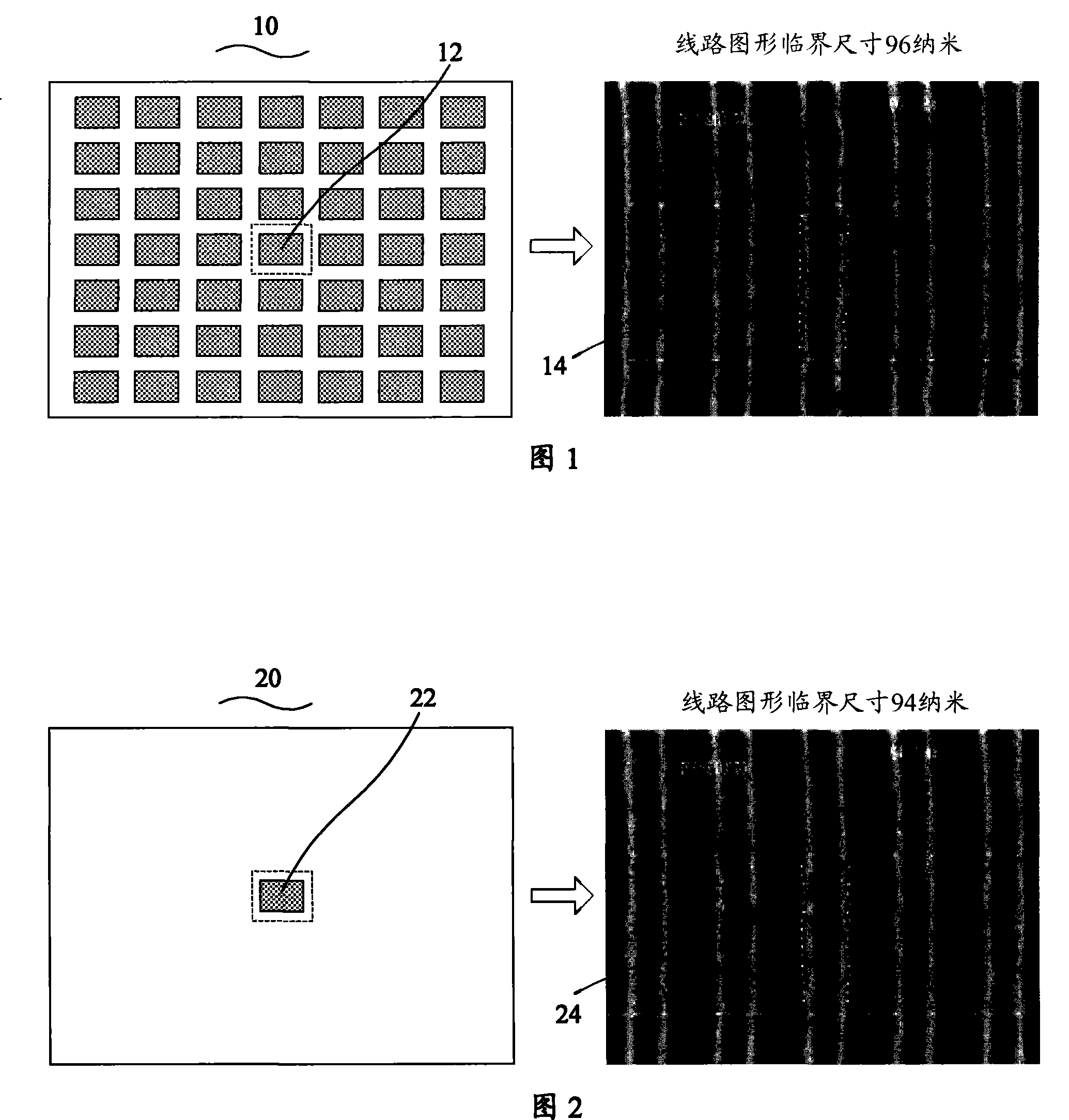
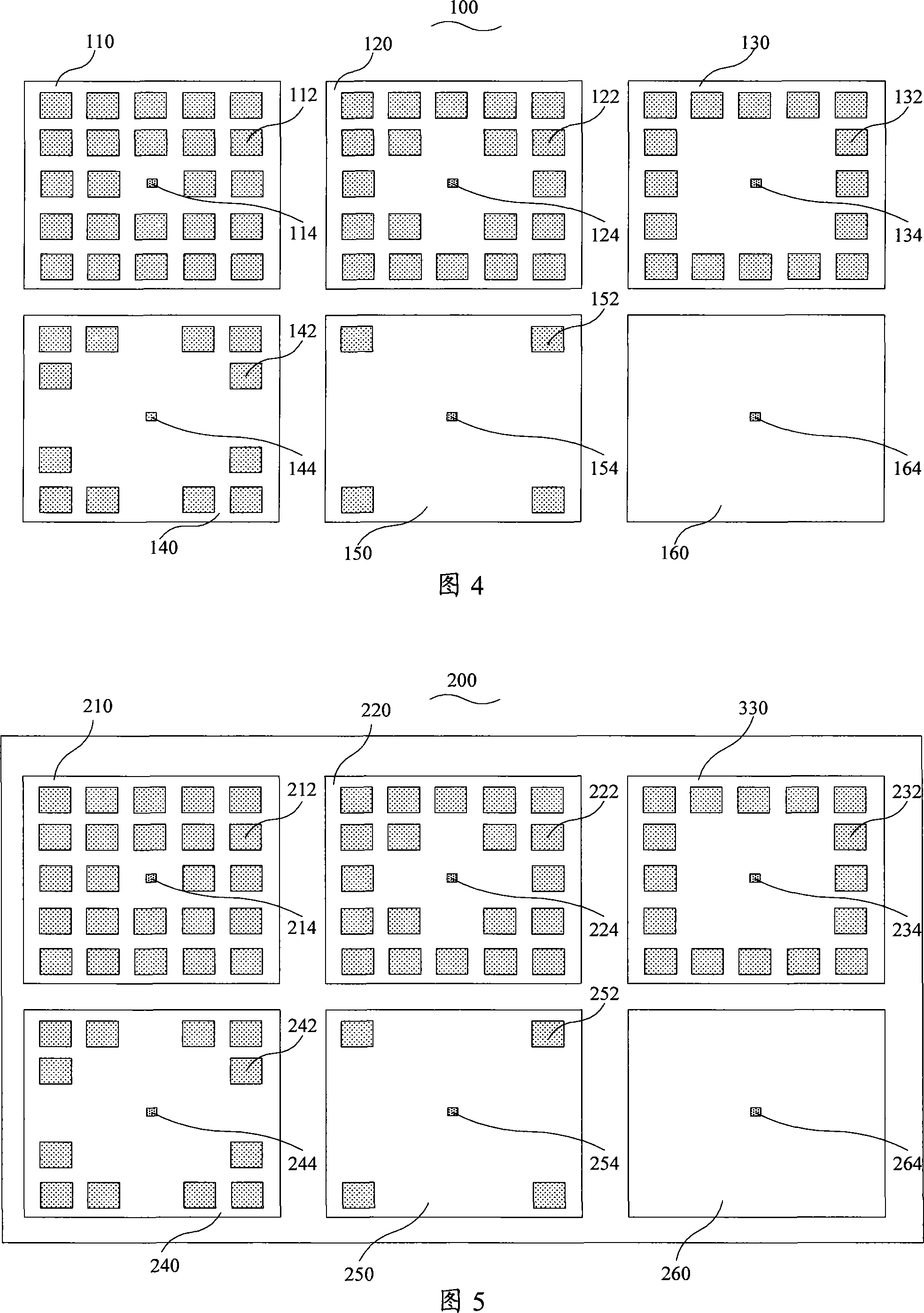
[0028] According to the density of semiconductor devices on the wafer, it can be divided into device dense area, device semi-dense area and device isolated area. The distance between the circuit patterns in the device dense area is equal to 1CD, and the distance between the circuit patterns in the device semi-dense area is greater than 1CD and less than Equal to 3CD, the distance between the circuit patterns in the isolated area of ​​the device is greater than 3CD.

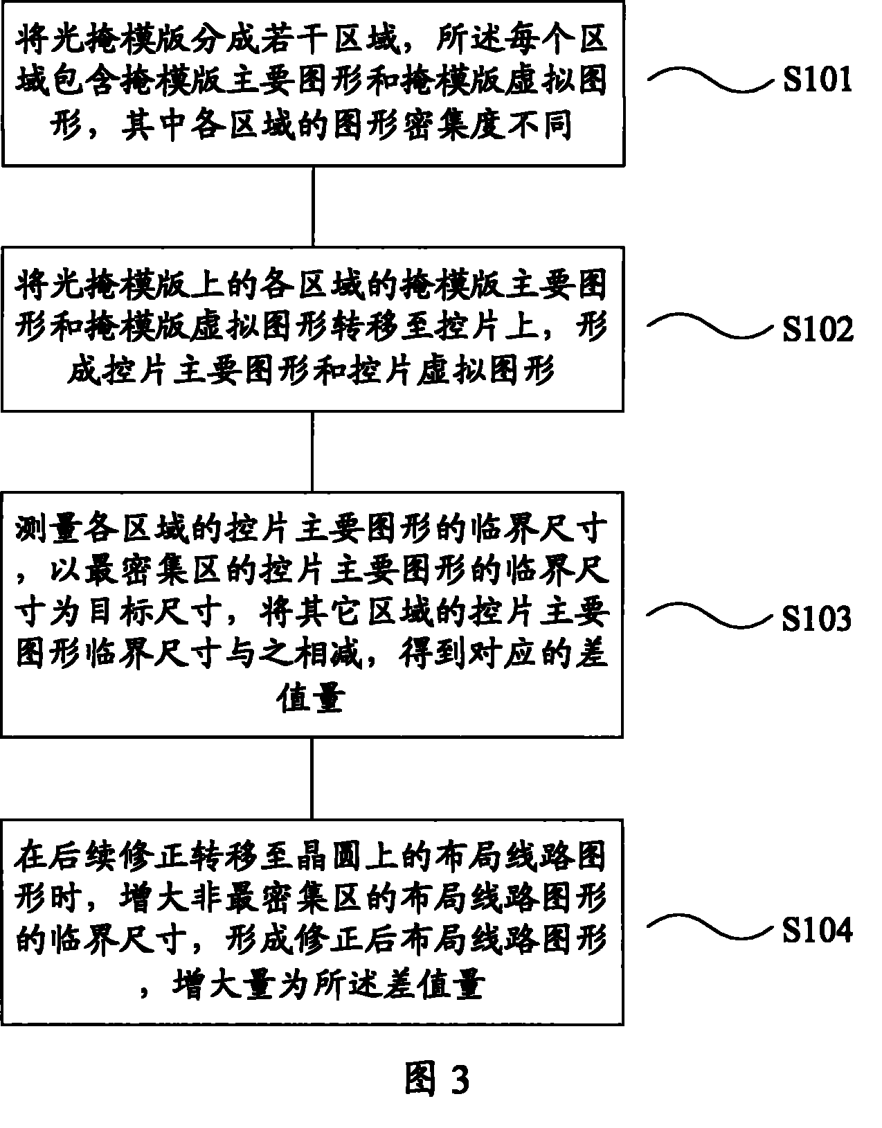
[0029] The invention divides the photomask plate into several regions with different pattern density; transfers the patterns of each region on the photomask plate to the photoresist film of the control sheet; measures the critical dimension of the photoresist main pattern in each region to obtain The critical size of the main graphics in the densest area is the target size, and the critical size of the main graphics in other areas is subtracted from it to obtain the difference; increase the critical size of the lay...


PUM

PropertyMeasurementUnit
critical dimensionaaaaaaaaaa

Abstract

The invention discloses a layout method, comprising the following steps: a photomask plate is divided into a plurality of regions, and each region includes a mask plate main pattern and a mask plate virtual pattern, wherein, each region has different pattern densities; the mask plate main pattern and the mask plate virtual pattern of each region on the photomask plate are transferred to a controlwafer so as to form a control wafer main pattern and a control wafer virtual pattern; the critical dimension of the control wafer main pattern in each region is measured, the critical dimension of the control wafer main pattern in the most dense region is taken as the target dimension to subtract the critical dimension of the control wafer main pattern in other regions, then the corresponding different value is calculated; the critical dimension of a layout line pattern in the non-most dense region is increased when subsequently correcting the layout line pattern transferred onto a wafer to form the corrected layout line pattern, wherein, the increased amount is the different value. The invention also provides a graphic and manufacturing method for the photomask plate. In the invention, the critical dimensions of the same line pattern transferred to the regions with different densities on the wafer are consistent.

Description

technical field [0001] The invention relates to the technical field of semiconductor manufacturing, in particular to a layout, a method for making and patterning a photomask. Background technique [0002] With the rapid development of semiconductor manufacturing technology, in order to achieve faster computing speed, larger data storage capacity and more functions of semiconductor devices, semiconductor chips are developing towards higher integration; and the higher the integration of semiconductor chips, Then the critical dimension (CD, Critical Dimension) of the semiconductor device is smaller. [0003] However, due to the impact of the resolution limit of the exposure tool (optical exposure tool), it is easy to produce the optical proximity effect ( OPE (optical proximity effect), such as right-angled corner rounded (right-angled corner rounded), line end shortened (line end shortened), and line width increase / decrease (line width increase / decrease) are common optical ne...

Claims


Application Information

Patent Timeline
Patent Type & Authority Patents(China)
IPC IPC(8): G03F1/00G03F1/14G03F7/00G03F1/36
Inventor 刘庆炜
Owner SEMICON MFG INT (SHANGHAI) CORP
Why Eureka
Try Eureka