Method for removing silicon oxide layer on surface of silicon substrate and contact hole forming

A silicon oxide layer, silicon substrate technology, applied in electrical components, semiconductor/solid-state device manufacturing, circuits, etc., can solve problems such as damage to the pattern shape, damage to the surface of the silicon substrate, etc., and achieve the effect of preventing damage

Inactive Publication Date: 2009-06-17
SEMICON MFG INT (SHANGHAI) CORP
View PDF1 Cites 10 Cited by
  • Summary
  • Abstract
  • Description
  • Claims
  • Application Information

AI Technical Summary

Problems solved by technology

However, this method may damage the surface of the silicon substrate, especially when a pattern is formed on the surface of the silicon substrate, it will damage the shape of the pattern

Method used


Image

  • Method for removing silicon oxide layer on surface of silicon substrate and contact hole forming
  • Method for removing silicon oxide layer on surface of silicon substrate and contact hole forming
  • Method for removing silicon oxide layer on surface of silicon substrate and contact hole forming

Examples


Embodiment Construction

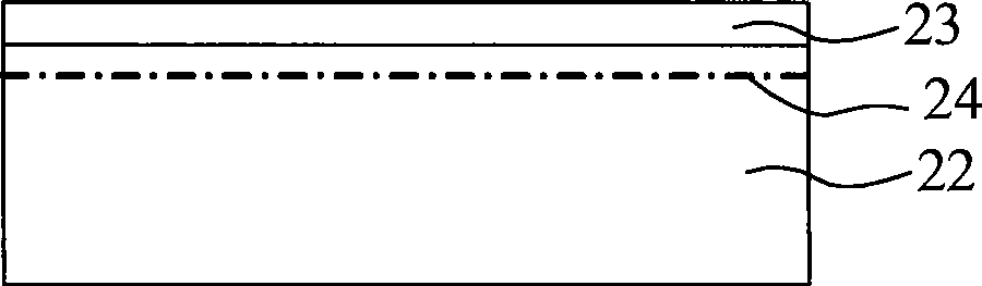
[0034] The invention provides a method for removing the silicon oxide layer on the surface of a silicon substrate, by converting the natural silicon oxide layer on the surface of the silicon substrate into ammonium fluorosilicate to passivate the surface of the silicon substrate, and then heating to make the ammonia fluorosilicate Chemicalization, the gas of ammonium fluorosilicate is pumped away, and the silicon oxide layer on the surface of the silicon substrate is removed.

[0035] refer to Figure 6 , the present invention at first provides a kind of method for removing silicon oxide layer on silicon substrate surface, comprises the steps:

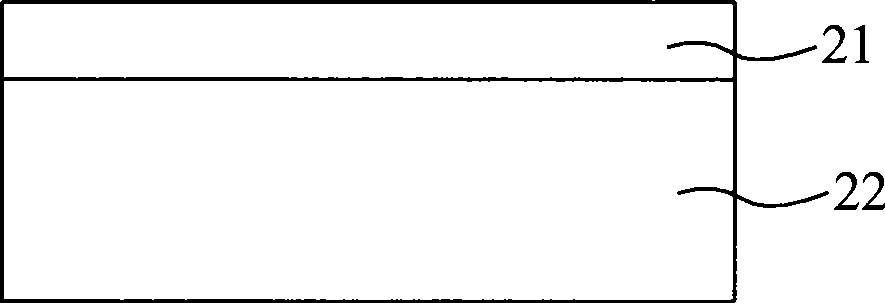
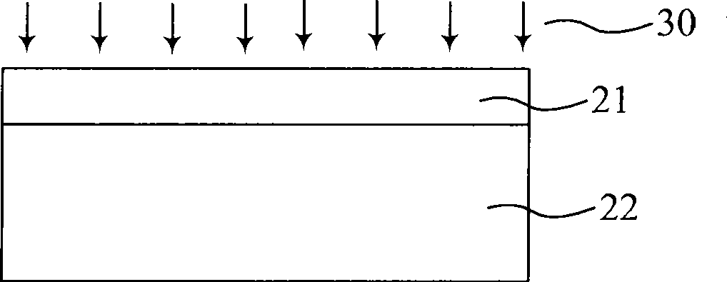
[0036] Execute step S101, put the silicon substrate with the silicon oxide layer into the etching equipment, the silicon oxide layer is formed on the surface of the silicon substrate, and the NH 4 F atomic group, which reacts with the silicon oxide layer on the surface of the silicon substrate to form a solid state (NH 4 ) 2 SiF 6 ...


PUM


Abstract

A method for removing silicon oxide layers from the surfaces of silicon substrates includes steps of disposing a silicon substrate with a silicon oxide layer into an etching device, wherein the silicon oxide layer is formed on the surface of the silicon substrate while NH4F atom groups formed in the etching device react with the silicon oxide layer on the surface of the silicon substrate to generate solid (NH4)2SiF6, and heating the silicon substrate to gasify the (NH4)2SiF6 on the silicon substrate, and exhausting the (NH4)2SiF6 gas from a heating device. Correspondingly, the invention further provides a method of forming contact holes. The method for removing silicon oxide layers from the bottom surfaces of silicon substrates prevents damages to the surfaces of the silicon substrates in the prior art by steps of transforming the natural silicon oxide layer on the surface of the silicon substrate into ammonium fluorosilicate which passivates the surface of the silicon substrate, then heating to gasify the ammonium fluorosilicate, exhausting the ammonium fluorosilicate gas and removing the silicon oxide layer from the surface of the silicon substrate.

Description

technical field [0001] The invention relates to the field of semiconductors, in particular to a method for removing a silicon oxide layer on the surface of a silicon substrate and forming a contact hole. Background technique [0002] In order to manufacture reliable semiconductor devices, it is necessary to control the surface properties of semiconductor substrates such as silicon. It is well known that when the silicon surface is exposed to a gas containing oxygen (such as air), a natural silicon oxide layer will be formed on the surface. This native silicon oxide layer must be removed before fabricating semiconductor devices. Moreover, the fabrication of semiconductor devices involves the formation of a silicon oxide layer on the silicon surface, and generally only the removed portion is desired to be removed to form circuit patterns. [0003] Usually CHF 3 gas or use C m f n and H 2 Removes the natural silicon oxide layer on the silicon surface. However, after using...

Claims


Application Information

Patent Timeline
Patent Type & Authority Applications(China)
IPC IPC(8): H01L21/3105H01L21/768H01L21/60
Inventor 何其旸
Owner SEMICON MFG INT (SHANGHAI) CORP
Why Eureka
Try Eureka