Wafer on-line detection method and on-line detection device

A detection device and detection method technology, applied in the direction of semiconductor/solid-state device testing/measurement, etc., can solve the problem of poor analysis accuracy of detection results, and achieve the effects of improving analysis accuracy, accurate judgment, and improved accuracy

Active Publication Date: 2009-06-17
SEMICON MFG INT (SHANGHAI) CORP +1
View PDF1 Cites 17 Cited by
  • Summary
  • Abstract
  • Description
  • Claims
  • Application Information

AI Technical Summary

Problems solved by technology

[0010] The present invention provides an online wafer detection method and an online detection device to improve the existing wafer detection method, wh

Method used


Image

  • Wafer on-line detection method and on-line detection device
  • Wafer on-line detection method and on-line detection device
  • Wafer on-line detection method and on-line detection device

Examples


Example

[0050] The first embodiment:

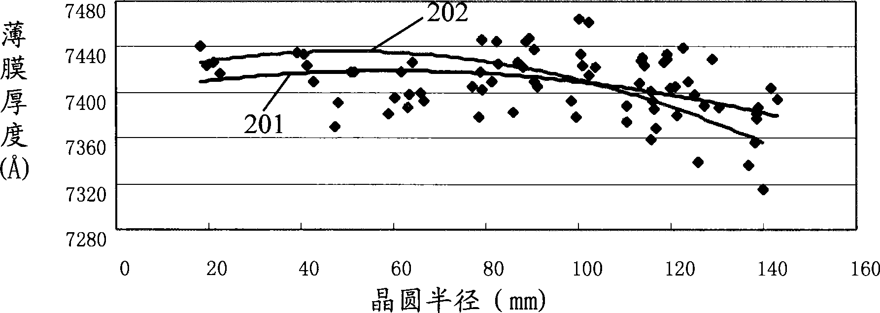
[0051] The first embodiment of the present invention introduces a new online wafer inspection method. The selection of inspection points is different from the traditional method, which can effectively improve the fitting curve of each inspection point data and the actual inspection data of the entire wafer. The degree of coincidence between the fitted curves.
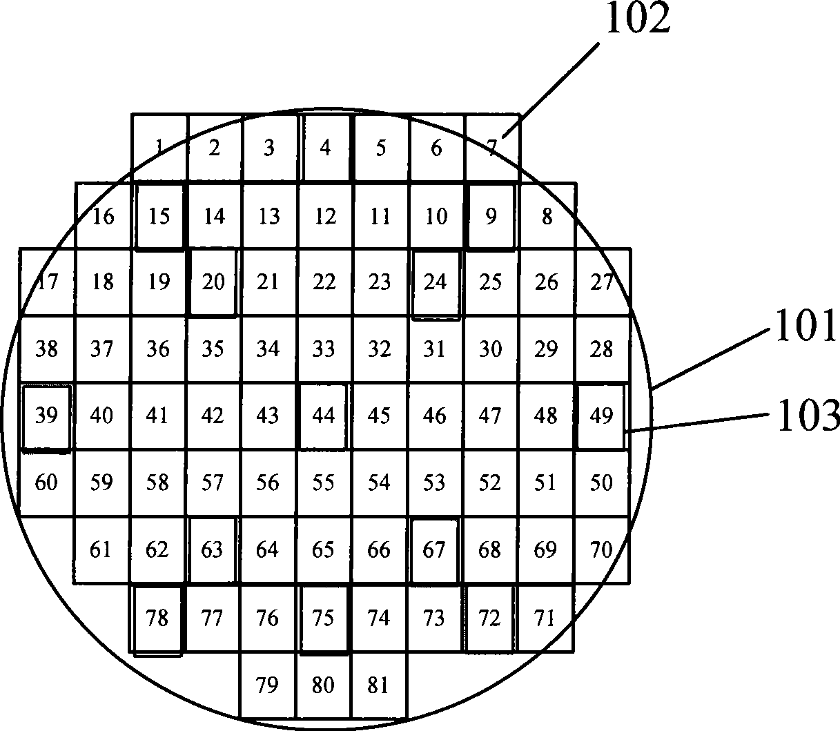
[0052] In the traditional wafer inspection method, the selection of each inspection point is determined according to the position distribution of each periodically arranged unit on the wafer, such as figure 1 As shown, usually 9 to 13 units are selected symmetrically with the wafer center as the center, and the distribution of the inspection results is obtained by testing the inspection area of ​​each selected unit, and the obtained distribution is used to derive the actual situation of the entire wafer Process conditions. However, practice shows that the data distribution of the inspection p...

Example

[0079] The second embodiment:


PUM


Abstract

The invention discloses a wafer on-line detecting method, the steps of the method comprise providing a to-be-detected wafer, wherein a plurality of units are periodically arrayed on the to-be-detected wafer, and each unit is internally provided with a detecting area, determining whether the detecting areas are in the corresponding units or not, determining the distribution of the detecting areas on the to-be-detected wafer according to the position of the detecting areas in the corresponding units, selecting a plurality of to-be-detected units according to distribution of the detecting areas on the to-be-detected wafer, detecting the detecting areas of the pluralities of to-be-detected units, and obtaining detecting data. The invention further discloses a corresponding wafer on-line detecting device, after utilizing the wafer on-line detecting method and the on-line detecting device of the invention, obtained detecting data can relatively accurately stand for the detecting data of the whole wafer, thereby increasing the analyzing accuracy of detecting results.

Description

technical field [0001] The invention relates to the technical field of semiconductor manufacturing, in particular to an on-line detection method and an on-line detection device for a wafer. Background technique [0002] The integrated circuit manufacturing process is a planar manufacturing process, which combines photolithography, etching, deposition, ion implantation and other processes to form a large number of various types of complex devices on the same substrate and connect them to each other to have a complete electronic functions. Wherein, a problem in any step of the process may lead to failure in the manufacture of the circuit. Therefore, in the prior art, on-line detection is often performed on the production results of each step of the process, such as on-line detection of the growth thickness of the film, the depth of etching, the accuracy of lithography overlay, etc., and the data obtained from the detection Carry out analysis to judge whether the process cond...

Claims


Application Information

Patent Timeline
IPC IPC(8): H01L21/66
Inventor 李健胡骏
Owner SEMICON MFG INT (SHANGHAI) CORP
Why Eureka
Try Eureka