Display device and method for production thereof

A technology for a display device and a manufacturing method, which is applied in the manufacture of semiconductor/solid-state devices, electrical components, and electrical solid-state devices, etc., can solve the problems of surface oxidation, inability to improve display quality, and unavoidable increase in energy consumption for auxiliary wiring, and achieve low energy consumption. consumption and improve display quality

Active Publication Date: 2011-07-27
SONY CORP
View PDF2 Cites 2 Cited by
  • Summary
  • Abstract
  • Description
  • Claims
  • Application Information

AI Technical Summary

Problems solved by technology

[0010] However, the technology disclosed in the above-mentioned Patent Document 1 has the disadvantage that if the electrodes on the drive panel are made of aluminum or an aluminum alloy, the auxiliary wiring made of the same material as the electrodes suffers from surface oxidation.
[0011] As described above, the prior art has difficulties in that an increase in power consumption cannot be avoided regardless of the structure of the auxiliary wiring, and that display quality cannot be improved by realizing a uniform voltage distribution in the electrodes on the light exit side.

Method used


Image

  • Display device and method for production thereof
  • Display device and method for production thereof
  • Display device and method for production thereof

Examples


no. 1 example

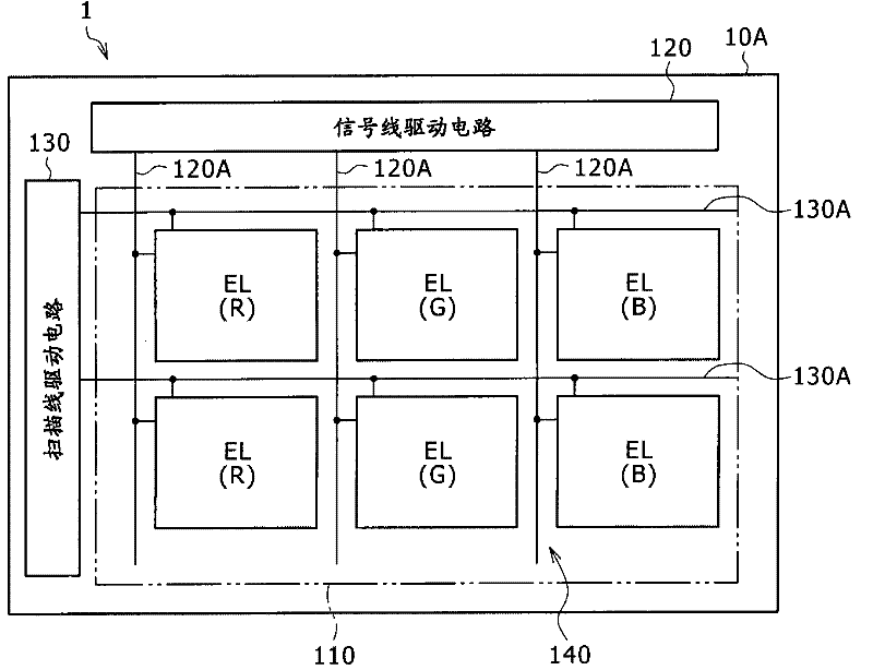
[0050] figure 1 is a view showing the structure of the display device (organic EL display device) of the first embodiment of the present invention. The organic EL display device 1 is a display device serving as an extremely thin organic color display device. The organic EL display device 1 includes a transparent substrate 10A and a plurality of organic EL elements (EL) arranged in a matrix on the transparent substrate 10A, thereby forming a display area 110 . The organic EL display device 1 also has a signal line driver circuit 120 and a scan line driver circuit 130 (both for displaying images) formed along the sides of the display region 110 .

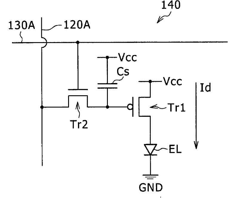
[0051] The display area 110 has a pixel driving circuit 140 formed therein. figure 2 is a view showing an example of the pixel driving circuit 140 . The pixel drive circuit 140 is an active type drive circuit formed under the first electrode 18A (to be described later), and includes a drive transistor Tr1, a write transistor Tr2,...

no. 2 example

[0100] A display device according to a second embodiment of the present invention will be described below. Constituent elements common to the first embodiment and the second embodiment are denoted by the same symbols, and their descriptions will not be repeated.

[0101] Figure 11 is a cross-sectional view showing the structure of the contact portion 25B of the display device (organic EL display device) of this embodiment. At the bottom of the contact portion 25B, there is a low-resistance wiring layer 26 on the transparent substrate 11A, and the low-resistance wiring layer 26 is on the same layer as the source signal line or the gate wiring connected to the thin film transistor Tr. The low-resistance wiring layer 26 has a thickness of 500 nm, and on the low-resistance wiring layer 26, the gate electrode 11, the gate insulating film 12, the silicon film 13A, the barrier insulating film 14 and n + type amorphous silicon film 13B. The low-resistance wiring layer 26 can preve...

no. 3 example

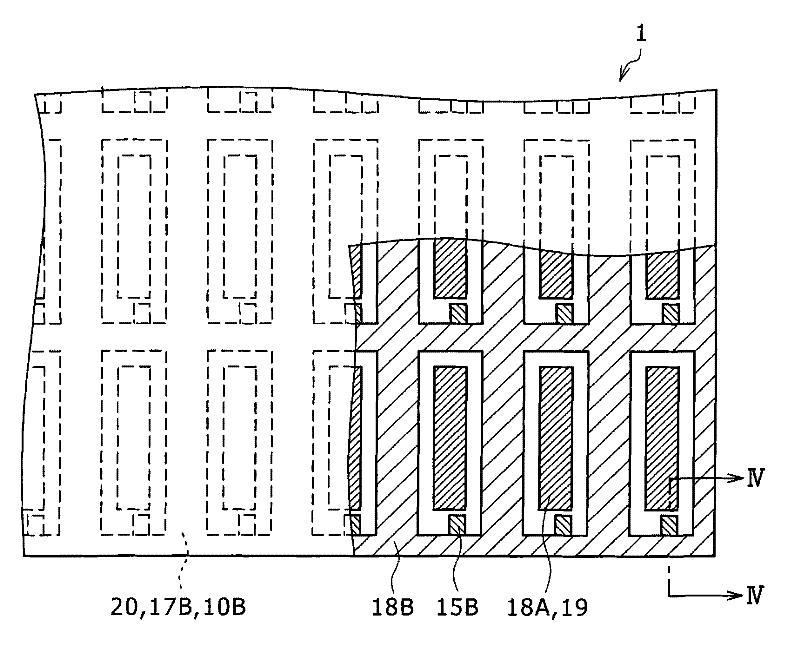
[0112] Figure 14 is a view showing the planar structure of the display region 110 of the organic EL display device 1 of the third embodiment of the present invention. Figure 15 is along Figure 14 Cross-sectional view taken along line XV-XV in . This organic EL display device 1 has the same structure as the organic EL display device of the first embodiment described above except that the auxiliary wiring 15C has the same layered structure as the contact portion 15B and is integrally formed with the contact portion 15B. Accordingly, corresponding constituent elements are denoted by the same reference numerals.

[0113] The present embodiment is similar to the first embodiment in that transparent substrates 10A and 10B, thin film transistor Tr, wiring layer 15A, contact portion 15B, protective insulating film 16, planarizing insulating film 17A, electrode insulating The film 21, the sealing resin 17B, and the organic EL element (EL).

[0114] The auxiliary wiring 15C is fo...


PUM


Abstract

The invention provides a display device and manufacturing method thereof. A display device having a plurality of driving elements and wiring parts electrically connected to the driving parts, includes: a plurality of first electrodes which are formed in correspondence to each driving element on the driving elements and the wiring parts; a plurality of light-emitting parts which are each formed onthe first electrodes; a common second electrode which is formed from a material that transmits light from the light-emitting part and is formed on the light-emitting parts; auxiliary wiring parts with a lower resistance than the second electrodes; and contact parts which are formed in laminate structure from a plurality of conductive layers and which electrically connect the second electrodes andthe auxiliary wirings with each other, with at least the lowermost conductive layer of the conductive layers of the contact parts being in direct contact with the second electrode. In the display device and manufacturing method in the invention, the second electrode and the auxiliary wiring parts are electrically connected to each other, thus, the contact resistance can not increase even the auxiliary wiring are superfically oxidized.

Description

[0001] Cross References to Related Applications [0002] The present invention contains subject matter related to Japanese Patent Applications JP 2008-123004 and JP 2007-326595 filed with the Japan Patent Office on May 9, 2008 and December 18, 2007, the entire contents of which are incorporated herein by reference Included here as a reference. technical field [0003] The present invention relates to a top emission type display device and a manufacturing method thereof. Background technique [0004] Recently, an organic EL display device that displays images by means of organic electroluminescence (EL, Electro Luminescence) is included in flat panel display devices that have attracted attention. The organic EL display device has a wide viewing angle and low power consumption because the display device utilizes the property that the organic EL element itself can emit light. Furthermore, since organic EL display devices have high responsiveness to high-definition high-speed ...

Claims


Application Information

Patent Timeline
Patent Type & Authority Patents(China)
IPC IPC(8): H01L27/32H01L23/522H01L21/82H01L21/768
CPCH10K50/824H01L27/1288H01L21/67075H01L2924/01013H10K50/814
Inventor 林直辉广升泰信藤冈弘文
Owner SONY CORP
Why Eureka
Try Eureka