Semiconductor encapsulation conformation throwing in multi-sinuosity connection finger

A semiconductor, zigzag connection technology, applied in the direction of semiconductor devices, semiconductor/solid-state device parts, electric solid-state devices, etc., can solve the problems of false contact of adjacent contacts, electrical short circuits, and different sizes of wafers in arrangement positions.

Inactive Publication Date: 2009-07-01
POWERTECH TECHNOLOGY
View PDF0 Cites 0 Cited by
  • Summary
  • Abstract
  • Description
  • Claims
  • Application Information

AI Technical Summary

Problems solved by technology

If other types of chips are selected, the arrangement position of the bonding pads of the chip or / and the size of the chip will be different, resulting in an oblique angle between the bonding direction of the bonding wire and the extending direction of the lead frame fingers or the interlacing of the bonding wires Problem, in the process of wiring and molding, it will accidentally touch adjacent fingers and cause an electrical short circuit

Method used


Image

  • Semiconductor encapsulation conformation throwing in multi-sinuosity connection finger
  • Semiconductor encapsulation conformation throwing in multi-sinuosity connection finger
  • Semiconductor encapsulation conformation throwing in multi-sinuosity connection finger

Examples


Embodiment Construction

[0071] In order to further explain the technical means and effects that the present invention adopts to achieve the intended purpose of the invention, below in conjunction with the accompanying drawings and preferred embodiments, the structure of a semiconductor package with multiple twists and turns for wire bonding proposed according to the present invention will be described in detail. Embodiments, structures, features and effects thereof are described in detail below.

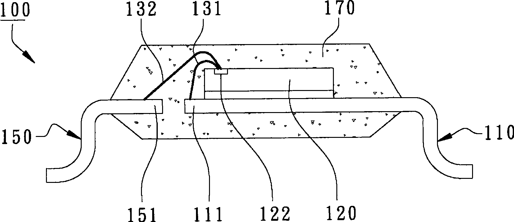
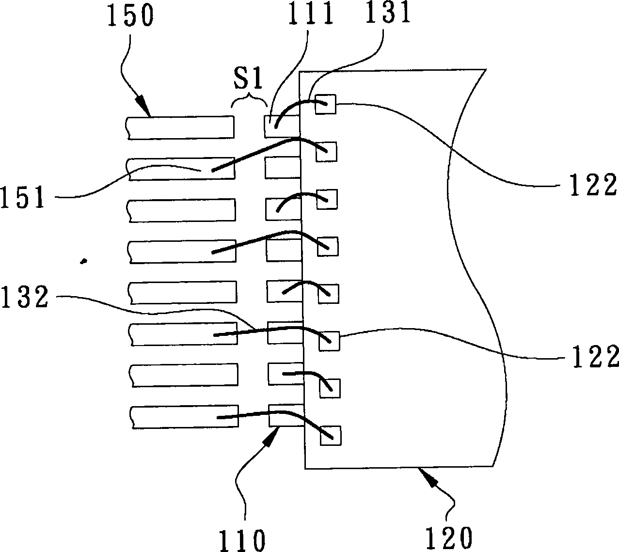
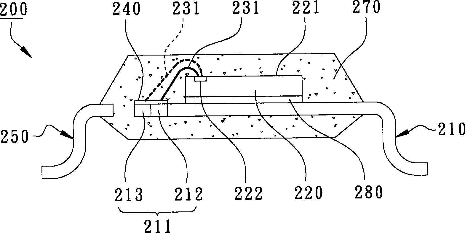
[0072] Figures 3 to 5 It is related to the first specific embodiment of the present invention, which discloses a semiconductor packaging structure in which wires are bonded to multiple fingers. image 3 A schematic cross-sectional view of the first pin is cut for the semiconductor package structure. Figure 4 A schematic cross-sectional view of the second lead is cut for the semiconductor package configuration. Figure 5 is a schematic plan view of the lead frame used in the semiconductor package structu...


PUM


Abstract

The invention relates to a semiconductor packaging structure of routing at multi-zigzag joint-fingers, mainly comprising a wafer, a plurality of pins of a wire holder and a plurality of welding wires for connecting the wafer and the pins. Each pin has a first joint-finger portion and a second joint-finger portion which are connected in zigzag, each end of the welding wires is connected with a welding cushion of the wafer and the other end is selectively connected with one group of the first joint-finger portions and the second joint-finger portions, which causes the routing direction of the welding wires to approximately align with the extending direction of the connected joint-finger portion, thereby being convenient for the routing process. Therefore, the packaging structure has community and can package wafers with different sizes or different allocations of welding wires, which can avoid false neighboring joint-fingers under the better angle of the joint-finger routing.

Description

technical field [0001] The invention relates to a semiconductor device, in particular to a semiconductor packaging structure in which wires are connected to fingers in many twists and turns. Background technique [0002] In known semiconductor package structures, the chip is mounted on a chip carrier, such as a lead frame or a circuit substrate. And commonly, a plurality of bonding wires formed by bonding are electrically connected to the chip and the chip carrier. Wherein, a plurality of fingers are provided on the chip carrier for connecting one end of the bonding wire. However, with the development of high-density integrated circuits, fine-pitch terminals, and the miniaturization of packaging volume, the arrangement gap and width of the fingers are getting smaller and smaller, making it easy for the bonding wires to touch adjacent fingers by mistake and cause an electrical short circuit. In addition, the distance for the fingers to cut off the welding wire is getting sm...

Claims


Application Information

Patent Timeline
IPC IPC(8): H01L23/488H01L23/49H01L23/495H01L23/498
CPCH01L24/48H01L2224/48091H01L2224/48247H01L2224/49433H01L2224/73265H01L2924/181H01L2224/32245H01L2224/48257H01L2224/49113H01L2224/05554H01L2924/14H01L2224/48H01L2924/00014H01L2924/00012H01L2924/00
Inventor 范文正徐玉梅
Owner POWERTECH TECHNOLOGY
Why Eureka
Try Eureka