Layout structure of circuit board

A layout structure, circuit board technology, applied in multi-layer circuit manufacturing, printed circuit components, etc., can solve the problem of increasing the equivalent impedance of transmission lines, the distance between transmission line segments cannot be increased, and the line thickness, line width and line spacing of transmission lines cannot be reduced And other issues

Inactive Publication Date: 2009-07-01
COMPAL ELECTRONICS INC
View PDF0 Cites 9 Cited by
  • Summary
  • Abstract
  • Description
  • Claims
  • Application Information

AI Technical Summary

Problems solved by technology

[0004] However, in order to increase the equivalent impedance of the transmission line segment with reference to the ground plane or power layer, the line thickness, line width and line spacing of the circuit board transmission line segment cannot be reduced due to the limitation of the accuracy and quality of the circuit board process.
Moreover, limited by the thinning of the circuit board, the distance between the transmission line segment and its adjacent reference plane cannot be increased
Based on the above factors, the current circuit board layout structure will be limited in design

Method used


Image

  • Layout structure of circuit board
  • Layout structure of circuit board
  • Layout structure of circuit board

Examples


Embodiment Construction

[0033] In the following two embodiments, the same reference numerals represent the same or similar components.

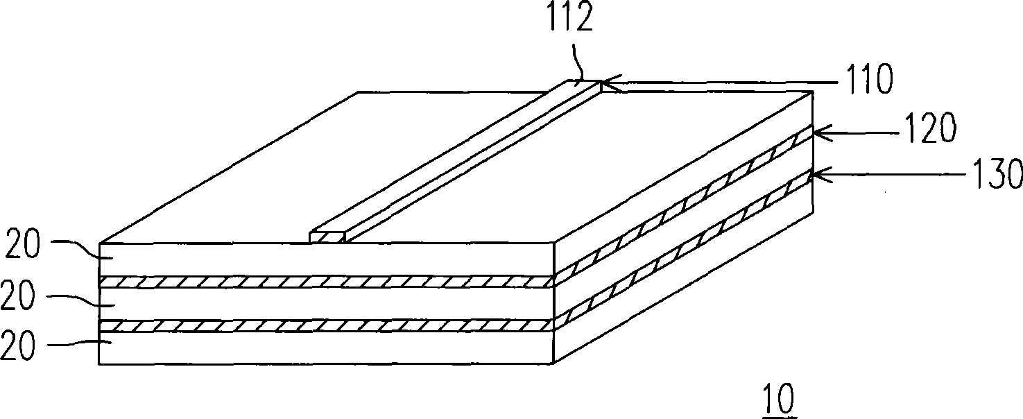
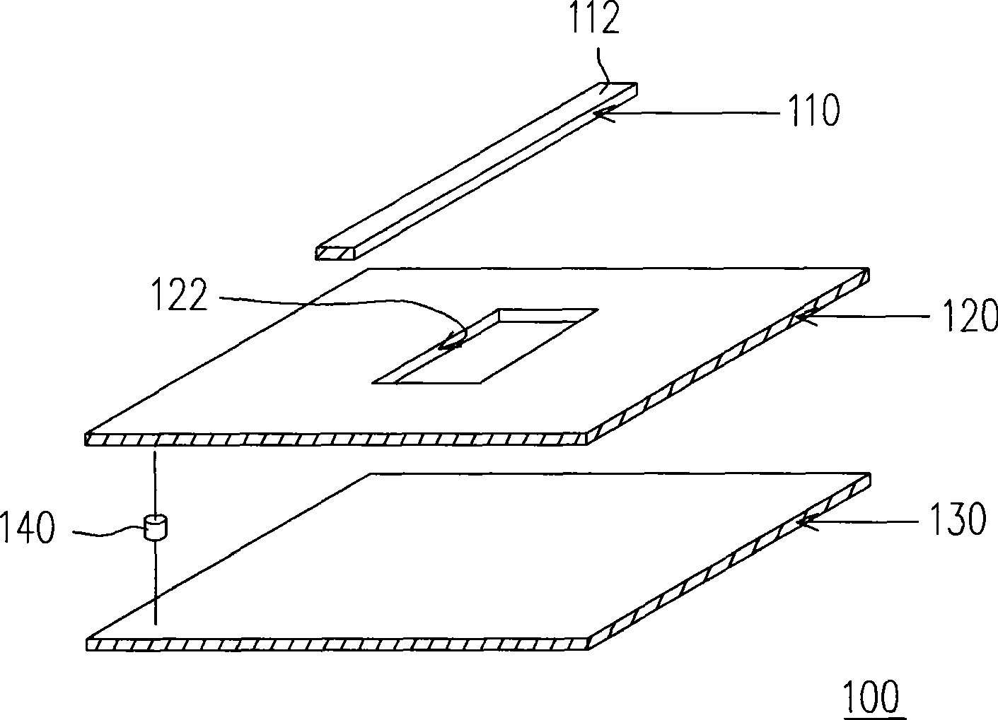
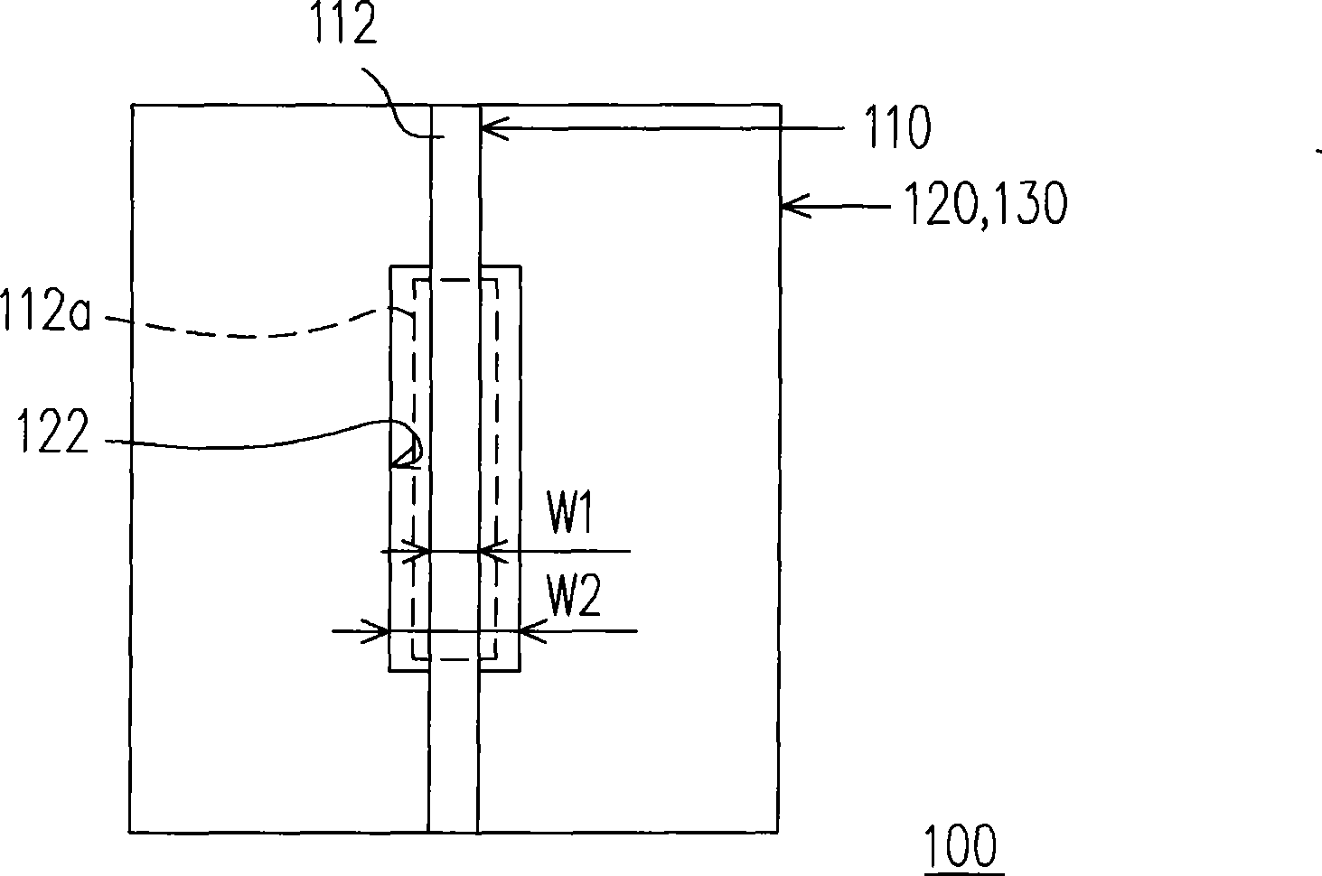
[0034] Figure 1A A circuit board layout structure illustrating an embodiment of the present invention is applied to a circuit board, Figure 1B draw Figure 1A An exploded view of the layout structure, Figure 1C draw Figure 1B A top view of the layout structure. Please refer to Figure 1A to Figure 1C , the circuit board 10 of this embodiment has a layout structure 100, which includes a first signal layer 110, a second signal layer 120 and a third signal layer 130, which overlap in sequence, and the second signal layer 120 is located at the first Between the first signal layer 110 and the third signal layer 130 . In addition, the circuit board 10 also includes a multi-layer dielectric layer 20, which is respectively located between these signal layers 110, 120 and 130 to electrically isolate these signal layers 110, 120 and 130, such as Figure 1A shown.

[...


PUM


Abstract

A layout structure of a circuit board comprises a first signal layer, a second signal layer and a third signal layer, wherein, the first signal layer is provided with a transmission line; the second signal layer overlaps with the first signal layer; the second signal layer is provided with an opening; the third signal overlaps with the first signal layer and the second signal layer; the second signal layer is positioned between the first signal layer and the third signal layer; the third signal layer is electrically connected with the second signal layer, and both the second signal layer and the third signal layer are ground planes or power supply layers; and the orthographic projection of a line segment of the transmission line on the third signal layer overlaps with the orthographic projection of the opening on the third signal layer. Therefore, the line segment of the transmission line is increased or reduced according to the equivalent impedance obtained by the second signal layer and the third signal layer.

Description

technical field [0001] The invention relates to a layout structure of a circuit board, and in particular to a layout structure of a circuit board which can change the impedance value at both ends of the same transmission line. Background technique [0002] Circuit boards have been widely used in various electronic devices. The circuit board can allow a plurality of electronic components to be installed on it, and these electronic components are electrically connected to each other through the circuit board's circuit, and part of the heat energy of these electronic components can be exported through the metal part of the circuit board. In practical application, the mainboard of a notebook computer is an application example in which many electronic components are mounted on a circuit board. [0003] In order to adjust the equivalent impedance obtained when both ends of a certain line segment of the transmission line of the circuit board refer to the ground plane or power plan...

Claims


Application Information

Patent Timeline
Patent Type & Authority Applications(China)
IPC IPC(8): H05K1/02H05K3/46
Inventor 许砥明
Owner COMPAL ELECTRONICS INC
Why Eureka
Try Eureka