Detection method and optical detection instrument for printed circuit board

A technology for printed circuit boards and optical detectors, which is applied in the directions of optical testing flaws/defects, instruments, and electrical measurement. It can solve the problems of heavy testing workload and complex IC solder pin identification and programming, and achieve the effect of simplifying the programming process.

Active Publication Date: 2009-07-08
深圳市泰视特测控技术有限公司
View PDF0 Cites 17 Cited by
  • Summary
  • Abstract
  • Description
  • Claims
  • Application Information

AI Technical Summary

Problems solved by technology

[0004] The present invention aims to provide a detection method and an optical detector for a printed circuit board, which can solve the problem that the existing optical detector for a printed circuit board needs to manually draw the test windows of the IC solder feet one by one when detecting the IC solder feet. Or by specifying the number of IC solder pins to array out the test window of the solder pins, the IC solder pin recognition programming is complicated, and the detection workload is relatively large.

Method used


Image

  • Detection method and optical detection instrument for printed circuit board
  • Detection method and optical detection instrument for printed circuit board
  • Detection method and optical detection instrument for printed circuit board

Examples


Embodiment Construction

[0027] The present invention will be described in detail below with reference to the accompanying drawings and in combination with embodiments.

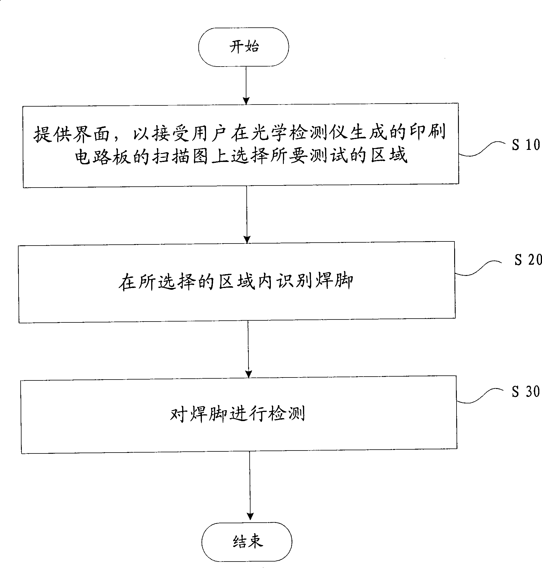
[0028] figure 1 A flow chart showing a method for detecting a printed circuit board according to an embodiment of the present invention includes:

[0029] Step S10, providing an interface to accept the user to select the area to be inspected on the scanned image of the printed circuit board generated by the optical detector, so that a frame can be programmed for a row of IC solder pins;

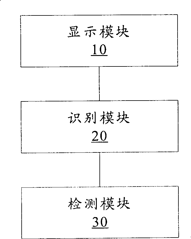
[0030] Step S20, identify the solder pins in the selected area, so that the number of IC solder pins and solder positions can be automatically identified by software;

[0031] Step S30, detecting the solder fillets.

[0032] This preferred embodiment can automatically identify the welding feet in the area selected by the user during detection, thereby solving the problem that the existing optical detector of the printed circuit board needs to manu...


PUM


Abstract

The invention provides a method for detecting printed circuit boards. The method comprises the steps of providing an interface to receive a to-be-detected area chosen on a printed-circuit-board scanning image generated through an optical detector by a user, recognizing a weld leg in the chosen area and detecting the weld leg. The invention also provides an optical detector for printed circuit boards. The invention solves the problems that the prior optical detector for printed circuit boards needs to manually draw test windows of IC weld legs one by one when the IC weld legs are detected or array the test windows of the weld legs through the quantity of the specified IC weld legs, and is complex to recognize and program the IC weld legs and high in detection workload, and then achieves the automatic recognition of a plurality of to-be-detected weld legs, as well as convenient fast effects. The method can greatly simplify the programming process for recognizing the IC weld legs in the use of AOI.

Description

technical field [0001] The invention relates to the field of printed circuit boards, in particular to a detection method and an optical detector for a printed circuit board. Background technique [0002] The printed circuit board optical detector is suitable for the detection of PCB (Printed Circuit Board, printed circuit board) defective products. Enterprise productivity and product quality. [0003] In the process of realizing the present invention, the inventor found that the existing optical detectors of printed circuit boards need to manually draw the test windows of IC solder pins one by one when detecting IC solder pins, or array by specifying the number of IC solder pins Out of the test window for solder pins, IC solder pin recognition programming is complicated, and the detection workload is relatively large. Contents of the invention [0004] The present invention aims to provide a detection method and an optical detector for a printed circuit board, which can ...

Claims


Application Information

Patent Timeline
Patent Type & Authority Applications(China)
IPC IPC(8): G01N21/88G01R31/02
Inventor 刘瑞祯熊光洁
Owner 深圳市泰视特测控技术有限公司
Why Eureka
Try Eureka