Setting method for photo-etching system NA-sigma

A lithography system and lithography technology are applied in the direction of photolithography for photomechanical processing of originals, optics, and patterned surfaces. It can solve problems such as reducing OPC efficiency, abnormal data processing, and OPC complexity. Achieve the effects of reducing complexity, improving correction efficiency, and saving data processing time

Inactive Publication Date: 2009-07-15
SEMICON MFG INT (SHANGHAI) CORP
View PDF0 Cites 6 Cited by
  • Summary
  • Abstract
  • Description
  • Claims
  • Application Information

AI Technical Summary

Problems solved by technology

[0006] The object of the present invention is to provide a method for setting NA-σ of a lithography system to solve the problem that the traditiona...

Method used


Image

  • Setting method for photo-etching system NA-sigma
  • Setting method for photo-etching system NA-sigma
  • Setting method for photo-etching system NA-sigma

Examples


Embodiment Construction

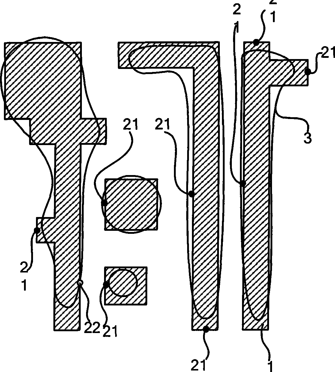
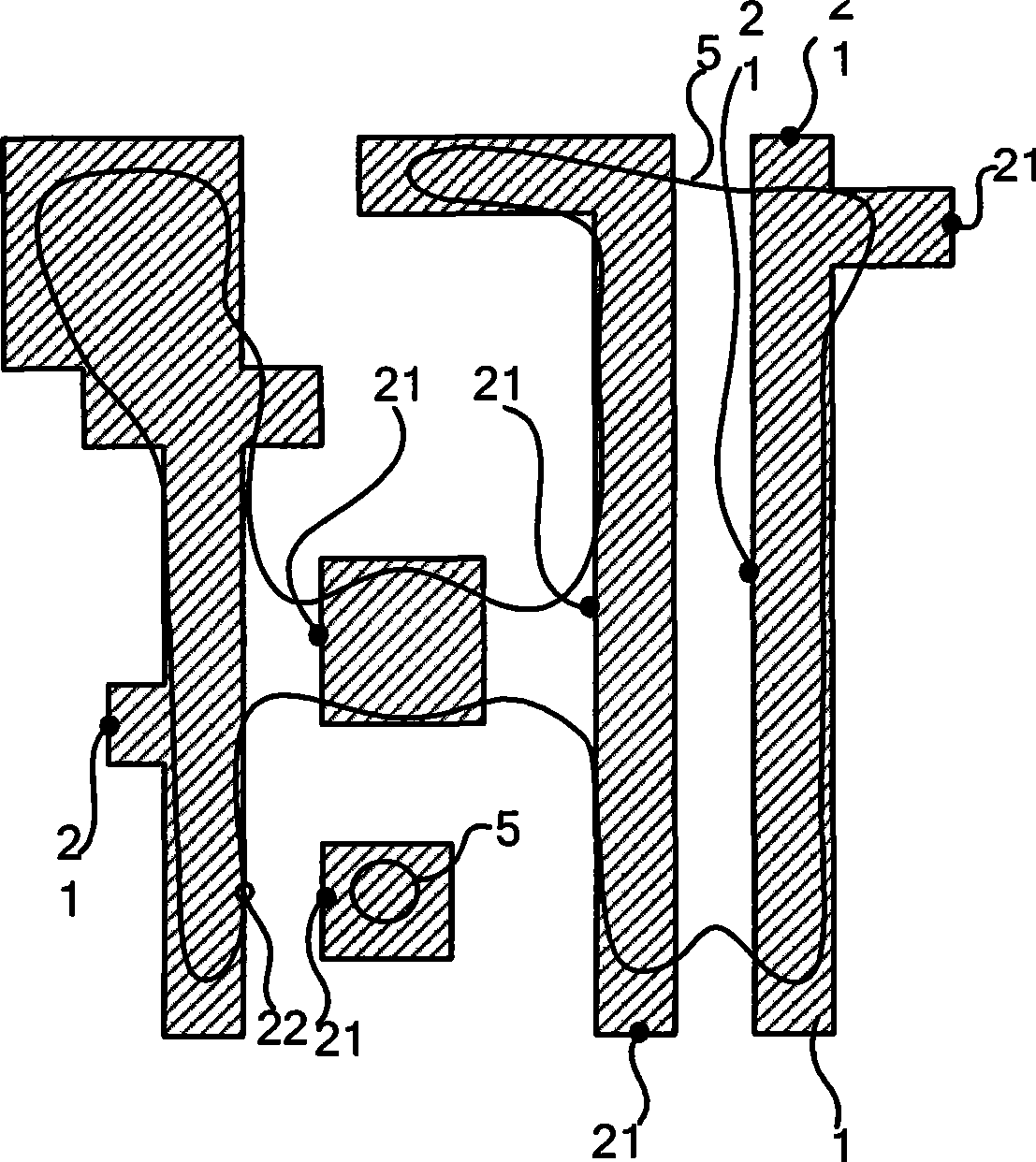
[0019] According to the traditional NA-σ setting method of the lithography system, a series of NA-σ values ​​of the lithography system with a larger lithography window for a design pattern with a certain feature size, ie, a larger M value, are obtained. For example, under the same NA value, one is a ring illuminator and the other is a quadrupole illuminator. The illuminator with these two different σ values ​​has a larger photolithographic process window when exposing a pattern of a certain feature size, that is, it is relatively small. Large M value. First, under a series of NA-σ setting values ​​of the lithography system obtained with a larger lithography window, several monitoring points are positioned according to a design pattern with a certain feature size. Generally speaking, to locate monitoring points is to locate these monitoring points according to some key parts in the pattern to be designed and the design characteristics of the pattern. see figure 1 , the design...


PUM


Abstract

The present invention provides a method for setting photolithography system NA-Delta, the NA-Delta value of the photolithography system can be further optimized under the photolithography system NA-Delta value with large photolithographic process window for avoiding reducing the subsequent OPC efficiency by the large EPE. The exposed design pattern can be calculated according to the NA-Delta value OPC model based on the design pattern and the photolithography system by positioning a plurality of monitoring points on the design pattern of certain characteristic dimension, then the EPE of the exposed pattern corresponding to the a plurality of monitoring points of the design pattern, when the calculated EPE value is minimum, the corresponding photolithography system NA-Delta value can be taken as the photolithography system NA-Delta value when exposing the design pattern of certain characteristic dimension. The method can ensure that the large photolithographic process window is provided when exposing the design pattern of certain characteristic dimension, meanwhile, the complexity of the subsequent OPC distribution pattern can be reduced, the abnormal OPC data can be reduced, and the OPC efficiency can be improved.

Description

technical field [0001] The invention relates to the field of selection and setting of parameters of a lithography device, in particular to a selection method for reducing two parameters of OPC (Optical Proximity Effect Correction) lithography system NA-σ in subsequent processes. Background technique [0002] In the semiconductor manufacturing process, photolithography equipment is used to expose different semiconductor device design patterns on its mask. In order to ensure the quality of the pattern imaged on the wafer (Wafer), when exposing these design patterns, set them according to the feature size (line width and minimum spacing between line widths) of the design pattern to obtain a larger process window (Process Window) The NA-σ value of the lithography system. The numerical aperture (Numerical aperture NA) of the imaging lens and the sigma (σ) value of the illuminator in the lithography system directly affect the process window during lithography and affect the quali...

Claims


Application Information

Patent Timeline
IPC IPC(8): G03F1/14G06F17/50G03F1/36
Inventor 李承赫
Owner SEMICON MFG INT (SHANGHAI) CORP
Why Eureka
Try Eureka