Template for forming solder bumps, method of manufacturing the template and method of inspecting solder bumps using the template

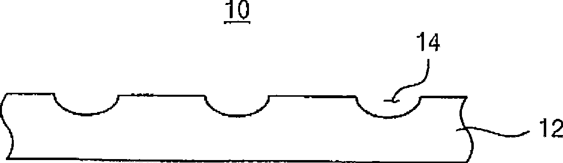
A solder bump and stencil technology, used in manufacturing tools, printed circuit manufacturing, semiconductor/solid-state device manufacturing, etc., can solve the problems of easily damaged stencil 10 and damage to the stencil, so as to facilitate detection and processing, prolong service life, and prevent damage. Effect

Inactive Publication Date: 2009-07-15
SECRON
View PDF5 Cites 0 Cited by
  • Summary
  • Abstract
  • Description
  • Claims
  • Application Information

AI Technical Summary

Problems solved by technology

Thus, the nozzle may damage the template 10 while injecting the soft solder
In addition, template 10 is prone to breakage during its transfer

Method used


Image

  • Template for forming solder bumps, method of manufacturing the template and method of inspecting solder bumps using the template
  • Template for forming solder bumps, method of manufacturing the template and method of inspecting solder bumps using the template
  • Template for forming solder bumps, method of manufacturing the template and method of inspecting solder bumps using the template

Examples


Embodiment Construction

[0028] The invention will be described in more detail hereinafter with reference to the accompanying drawings showing embodiments of the invention. However, this invention may be embodied in many different forms and should not be construed as limited to the embodiments set forth herein. Rather, these embodiments are presented so that this disclosure will be thorough and complete, and will fully convey the scope of the invention to those skilled in the art. Like numbers refer to like elements throughout the specification.

[0029] It will be understood that when an element is referred to as being "on" another element, it can be directly on the other element or intervening elements may be present. In contrast, when an element is referred to as being "directly on" another element, there are no intervening elements present. As used herein, the term "and / or" includes any and all combinations of one or more of the associated listed items.

[0030] It should be understood that alt...


PUM


Abstract

A template for forming solder bumps includes a transparent substrate on which a plurality of cavities is formed at an upper surface portion thereof, and a light-reflective layer and a protective layer formed on a lower surface of the transparent substrate. When a nozzle makes close contact with the template to inject a molten solder into the cavities, damage to the template may be prevented by the light-reflective layer and the protective layer, and thus the lifetime of the template may be increased. An inspection process on the solder bumps, which are formed in the cavities of the template, may be easily performed by analyzing light reflected by the light-reflective layer.

Description

[0001] Cross References to Related Applications [0002] This application claims priority under 35 U.S.C. §119 from Korean Patent Application No. 2008-1790 filed with the Korean Intellectual Property Office on January 7, 2008, the contents of which are hereby incorporated by reference in their entirety. technical field [0003] The present invention relates to a template for forming solder bumps, a manufacturing method of the template, and a method of inspecting solder bumps using the template. More particularly, the present invention relates to a stencil having cavities for forming solder bumps in a microelectronic packaging process, a method of manufacturing the stencil, and a method of inspecting the solder bumps formed in the cavities of the stencil. Background technique [0004] Recently, the interconnection method in the microelectronic packaging process has gradually changed from wire bonds to solder bumps. There are various solder bump fabrication techniques used i...

Claims


Application Information

Patent Timeline
Patent Type & Authority Applications(China)
IPC IPC(8): H01L21/60H01L21/66B23K3/06
CPCH05K2203/0338H01L21/6835H05K1/0269H01L2224/16H05K3/3478H01L2924/01078H05K2203/0113H05K2203/163H05K2201/0108H01L2224/11003
Inventor 朴泌奎
Owner SECRON
Why Eureka
Try Eureka