Solar cell and method for manufacturing the same

A solar cell and electrode technology, applied in the field of solar cells, can solve problems such as damage to the emitter, solar cell fill factor or energy conversion efficiency deterioration, etc., and achieve the effects of preventing shunt, excellent energy conversion efficiency, and filling factor improvement.

Inactive Publication Date: 2009-07-29
SAMSUNG SDI CO LTD
View PDF0 Cites 8 Cited by
  • Summary
  • Abstract
  • Description
  • Claims
  • Application Information

AI Technical Summary

Problems solved by technology

In this way, during the sintering process, the paste used to form the electrodes on the rear surface of the semiconductor substrate and the inner wall of the via hole may damage the emitter, thereby causing a shunt or a short circuit, thereby affecting the fill factor or energy conversion efficiency of the solar cell. become worse

Method used


Image

  • Solar cell and method for manufacturing the same
  • Solar cell and method for manufacturing the same
  • Solar cell and method for manufacturing the same

Examples


experiment example

[0088] A p-type silicon semiconductor substrate having a thickness of 240 μm and including via holes with a diameter of 100 μm was formed. This semiconductor substrate has minute protrusions and recesses formed by texturing. Phosphorus oxychloride (POCl 3 ) was pyrolyzed in a diffusion furnace, a phosphosilicate glass (PSG) layer with a thickness of 0.5 μm was formed on the surface of this semiconductor substrate, and phosphorus in the PSG layer diffused into the semiconductor substrate to form an emitter portion. PSG was removed by dilute hydrofluoric acid (HF), and the unwanted portion of the phosphorus-diffused fraction was removed by potassium hydroxide (KOH) solution.

[0089] An antireflection layer composed of silicon nitride and having a thickness of 75 nm was formed on the front surface of the semiconductor substrate by plasma enhanced chemical vapor deposition.

[0090] A paste for forming the silver-containing first electrode portion is applied on the front surfac...


PUM


Abstract

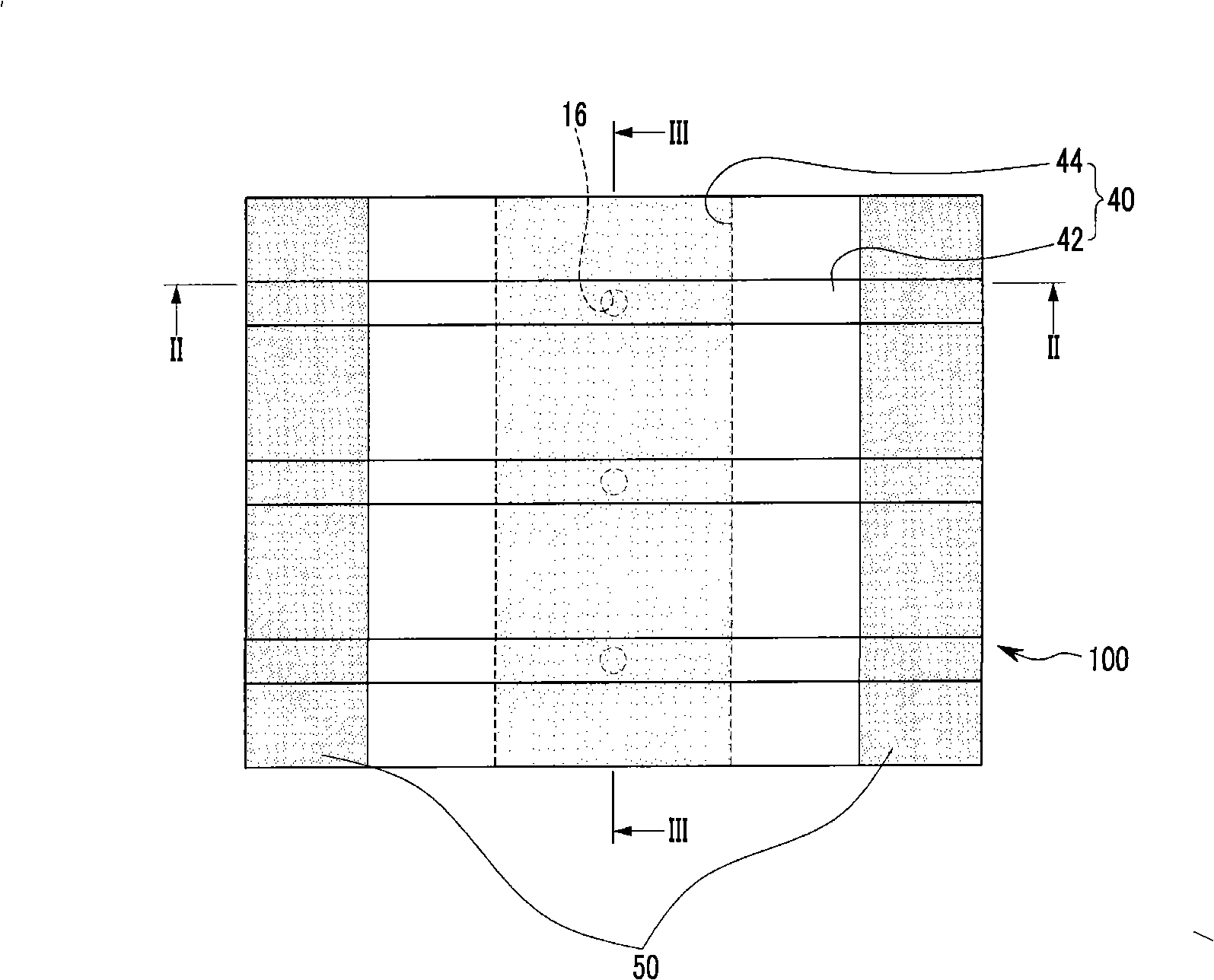
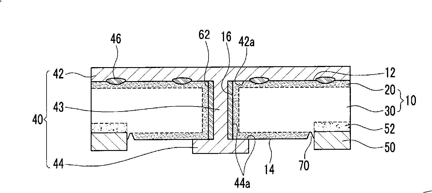
A method for manufacturing a solar cell having an improved process and a solar cell manufactured by the method include a semiconductor substrate having a via hole, an emitter portion, a base portion, a first electrode, and a second electrode. The emitter portion and the base portion form a p-n junction in the semiconductor substrate. The first electrode is electrically connected to the emitter portion, and the second electrode is electrically connected to the base portion. Conductive crystals are formed to electrically connect a first electrode portion of the first electrode and the emitter portion to increase the efficiency of the solar cell.

Description

technical field [0001] Aspects of the present invention relate to solar cells and methods of manufacturing the same. More particularly, aspects of the present invention relate to a method of manufacturing a solar cell with an improved process and a solar cell manufactured by the method. Background technique [0002] Solar cells generate electricity from the sun. Solar cells are environmentally friendly and provide a nearly unlimited source of energy. In addition, solar cells have a long life. According to the scheme of generating electricity using solar energy, examples of the solar cell include a semiconductor solar cell and a dye-sensitized solar cell. [0003] In a semiconductor solar cell, a base portion and an emitter portion are formed in a semiconductor substrate having different conductivity types to form a p-n junction. The first electrode is electrically connected to the emitter portion, and the second electrode is electrically connected to the base portion. A...

Claims


Application Information

Patent Timeline
Patent Type & Authority Applications(China)
IPC IPC(8): H01L31/068H01L31/0224H01L31/18H01L31/04H01L31/06
CPCH01L31/022425H01L31/03529Y02E10/50Y02E10/547H01L31/02245H01L31/06
Inventor 文仁植金大园
Owner SAMSUNG SDI CO LTD
Why Eureka
Try Eureka